|
Ascel Æ20401 5.8 GHz Frequency Counter/Power Meter Build |
Æ20401 5.8 GHz Frequency Counter/Power Meter Build
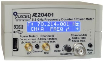
The time has come for yet another kit-build article. This time it is the Ascel Electronic Æ20401 5.8GHz Frequency Counter and Power Meter (pictured above). This device is another offering from Ascel Electronic (www.ascel-electronic.de) who, you may recall, produced the highly accurate Æ20204 LC Meter about which I wrote in a previous article. The current project, the Æ20401 has the same form factor as the Æ20204. It is a safe bet that this entire device family will share the same enclosure size and type. The other devices in this family are the Æ20218 Milliohm Meter and the Æ20125 10 MHz Sweep DDS Function Generator. From my experience with this product line, I believe it to be a well-designed and highly functional line of devices.
The Æ20401 combines three different functions :
It can measure Frequency/Period (Channel A/B) and RPM (Channel A). The number of pulses per revolution is adjustable via software of front panel controls. The Offset and Smooth functions and the selectable Trigger Edge capability further extend the possible applications.
The USB interface allows remote control of the frequency counter through the Windows® software that is included with the kit. The easy, plain text command protocol allows simple integration with external tools and systems. Each and every command or operational function of the Æ20401 can be software-controlled.
The circuit diagram (Figures 2 & 3) of the Æ20401 is best divided into several operational sections, as described below. Larger views of the schematics are at the end of this article.
The digital section, based on IC1 (an Atmel ATmega328 microcontroller or µC) controls all functions, computes displayed meter readings, and drives the LCD. The USB port is handled by the Windows®-friendly FT230X UART-USB Bridge (IC5), which is a surface-mount device and as such is pre-installed if the USB interface option is ordered. I say “Windows®-friendly” because the FT230X is an implementation of the FTDI USB chipset, which is known to be readily compatible with all versions of Microsoft Windows®. IC8, in a TO-92 three-pin package, is the 2.5VDC reference for the ADC (analog to digital converter) that is used to convert the analog output of the Power Meter Module into a digital value for further processing and display.
The +5VDC digital supply is developed in the linear voltage regulator IC4, a ubiquitous 7805 three-pin voltage regulator IC. Diode D1 protects IC4 from reverse polarity of the input voltage to the voltage regulator. Decoupling capacitors are placed next to all IC’s. Each optional add-in module has its own power regulation and decoupling capacitors on its own printed circuit board (PCB).
Considering the Channel A/C input circuitry, the DC offset is removed from the input signal first, with the signal then being impedance-matched and directed to the input amplifier. Diodes D2 and D3 limit the signal in case of input overload, setting the maximum signal level to approximately 700mV or the value of the forward voltage drop of a single standard silicon diode. The 10K? front panel Sensitivity potentiometer P1 is used to attenuate the signal. An LT1016 high-speed comparator (IC6) with hysteresis is then used to compare the signal against a reference voltage.
A 5VP-P square wave of the same frequency as the input signal is present and can be processed by the digital logic IC’s. Taken together with the Channel B input signal, which is already divided by 500 in the Channel B module, it is divided by 2 by IC2, a 74ACT74 high-speed quad flip-flop, and then is divided again, this time by 8, through the action of IC3, a 74HC393 dual 4-bit counter IC.
All of these signals are then directed to IC7, a 74HC1543 multiplexer IC, where three signals are present, which are the comparator output from Channel A, the divided-by-16 signal, and the divided-by-1000 signal from Channel B.
Depending upon the selected active channel and mode, the ATmega328 µC selects one of these signals which is then processed to create a reading for display on the LCD panel and in the software if so connected.
The analog output from the Power Meter (Channel PWR) is converted to a digital value by the µC's internal ADC. This digital value is then used to calculate the power reading for display.
3.3VDC is needed for the internal operation of the Channel B module. To develop that supply voltage, voltage dividers on the data lines, consisting of R17 & R19, R23 & R20, and R22 & R21 are employed to reduce the amplitude from 5VD to 3.3VDC. R15 and the D4 & D5 diode combination serve to limit the external signal input (EXT) from an overvoltage condition.
The Æ20401 can be ordered with either the standard 20MHz crystal oscillator for the CLK function, or the optional Æ204011 1ppm TCXO Module.
R2, a 2-watt resistor, is capable of withstanding short overloads on Channel A/C without damage. However, it is very important that the maximum specified input level limits not be exceeded so as higher to not cause damage to the frequency counter.
Only one surface mount device (SMD) is utilized in the Æ20401, and then only when the optional USB interface is ordered. This chip, the FT230X mentioned earlier, is pre-installed on the PCB, helping to make this kit more friendly for less-experienced kit builders, as well as making the build easier for experienced builders.
The comprehensive manual should help answer all questions that may arise during assembly, but does not quite reach that goal – more about that later on. Certain specific components are installed to the foil side of the printed circuit board (PCB), and are so identified in the parts list by the placement of an asterisk (*) next to the part identifier.
Ascel makes the assertion on their website that all parts and components needed for this build are included, but this is patently not a true statement. What is not included with this kit, as I noted in my previous article on the Ascel Æ20204 LC Meter, are the lengths of hook-up wire required to connect the rear panel components into the circuits, and four rubber feet for the underside of the enclosure. Once again, this is no problem for me, as I normally have large quantities of both wire and rubber feet in stock and ready for use.
As I will explain in detail later, this build did not go as smoothly as it could have, due to two failed components. Yes, I said two, for one of which I will accept partial potential responsibility. The second one was a fluke and was very strange indeed… but more about that later.
Let’s take a few minutes to talk about costs. As expected with a device of this capability, while the price is not a bank-breaker, it is none the less not exactly cheap. Here is how the cost broke out, all in US dollars :
I ordered my unit with all of the available options, and with the blue and white LCD panel. I like the blue and white display, as I think that it is easier on the eyes than is the yellow and green display. The total price of the unit as ordered was $269.15; the shipping was an additional $13.20 for a delivered total of $282.35. Note that the enclosure is a required “option” when the optional frequency and/or power modules are installed. This is because the front panel is an integral component of the structural support system for these add-in modules. The lead time on this item was about three weeks from order to delivery. The unit came in well-packaged and with the various add-in modules each sealed into its own anti-static pouch. The main group of PCB components were all together in a single anti-static pouch, together with the printed circuit board in its own plastic bag.
The assembly of this kit is pretty much a straight-forward event, with the caution that the builder must take special care in placing each component in its assigned location. The PCB is quite crowded, with all resistors installed on end. Silk-screened legend and location outlines are present on the PCB, but due to the close proximity of many of the components, it can be a bit confusing as to which label goes with which outline. To aid in this a little bit, the manual includes a grid-type component map (Figure 7) in which the PCB is divided by a grid in which each location is identified by distances in millimeters from the upper left corner of the PCB. This is accompanied by a component list in which each component is identified as to its location by a pair of distances, one on each of the horizontal or “X” and vertical or “Y” axes. Thus, a component listed as being “26x13” (as is capacitor C10) would be 26mm in from the left edge and 13mm down from the top edge. In this diagram, the PCB is oriented such that the BNC jack is at the upper left of the PCB.
There is no step-by-step assembly guide in the manual. It is expected that the kit builder can read a schematic and follow the grid-square guide and silk-screen legend to achieve a successful build. The common methodology of installing components in the order of their profile heights, lowest to highest, will serve the builder well. Some points that require special attention are the following :
As always, resistor values can be ascertained by use of the color-coded stripes on the resistor bodies, but if the builder is unsure, an ohmmeter or universal component tester will help. Another area of concern is the installation of the optional Æ204011 1ppm TCXO in place of the standard 20MHz crystal oscillator at the CLK position. It is important that Pin 1 of the oscillator is aligned with the Pin 1 location on the PCB, as indicated by the silk-screen legend. Pin 1 of the 20MHz crystal oscillator is identified by a dot in one corner of the oscillator case, but in the case of the Æ204011 1ppm TCXO, Pin 1 is identified by a silk-screened “1” on the underside of the oscillator PCB, and by the fact that the only sharp corner on the oscillator PCB is the Pin 1 corner (Figure 8).
I normally socket all IC’s during a build unless there is a space or circuit design reason not to do so. In the case of the Æ20204, space is not an issue, but circuit design is. At the frequencies potentially encountered herein, the added length of the IC socket leads could become problematic. As a result, the only IC that is socketed is the ATmega328 µC, for which the kit maker supplies a socket.
When assembling this PCB (Figure 9), care must be taken to ensure that there are no solder bridges and/or cold or dry solder joints, which of course is always the case. However, with this unit, it becomes a bit more difficult to correct if the builder should need to go back and do so. This is because the LCD panel, when installed (Figure 10), will cover most of the solder points on the main PCB, and any required rework of the main PCB solder points will require the desoldering and removal of the LCD panel. I had to do just that during my build experience.
A necessary step of the build process involves adjustment of the input amplifier, after warming up the TXCO for at least thirty minutes. In attempting to make the adjustment, I found that there was no signal getting to Pin 3 of the LT1016 comparator (IC6), as there should have been.
Adjustment of the input amplifier is best done by inputting a sine wave (25kHz at 100mVP-P) into the BNC jack, and then reading the waveform at IC6 Pin 3. That waveform is adjusted to be centered at the 0V line in the oscilloscope using the vertical position control. Then, without changing that vertical position setting, the square wave at IC6 Pin 2 is read, and is adjusted to that same centered position by carefully adjusting the 200? trimmer potentiometer (R2). In my build, the sine wave was not present at IC6 Pin 3, so I had to figure out why it was missing.
A little bit of tracing of the signal with the oscilloscope showed that it was present at the gate of T1, the BF256A J-MOSFET, but was not present at the MOSFET’s source pin. MOSFET’s are extremely sensitive to static electricity and are easily damaged by such static discharges. I had been reasonable careful when handling the FET, so I cannot say that I take full blame for its failure, but that’s a moot point anyway. What mattered was that I had to replace the FET, which I was able to do easily, as I had stock on that device type.
I set about desoldering and removing the LCD panel, which was relatively easy given the capability of the solder station that I use, which is the same as the one that is on the club’s test and repair bench. So, it did not take very long to get the LCD panel off (Figure 11) and to replace the FET. I decided to attempt to make the input amplifier adjustment before re-installing the LCD panel, as I did not need to use the panel for anything during the adjustment process. As luck would have it, that was a smart move on my part, as it turned out that I had to make another repair before the unit would adjust up properly.
Having reconnected the signal generator and gotten the oscilloscope ready, and having waited out the requisite half-hour warm-up period for the TCXO, I again attempted the adjustment. This time, I had the signal at IC6 Pin 3, but adjustment of the R2 200? trimmer pot had no effect - there was no square wave at Pin 2 of IC 6. Back to the drawing board.
After the better part of an hour of poking, probing measuring, and thinking, I found that there was an open in the 200? trim pot. There was no continuity between the wiper and either end of the resistive element. The resistive element had proper continuity and the correct resistance through it, but the pot was open between either end and the wiper terminal. Fortunately, I had a suitable trimmer pot in stock, so this too was a quick repair. Finally, after again going through the TCXO warm-up period, I was able to properly adjust the input amplifier and bring the unit to life.
I said earlier that adjustment of the unit’s input amplifier is “best done” by inputting a sine wave and using an oscilloscope to read the signals at Pins 2 and 3 of IC6. There is an alternative method of making this adjustment, which is useful for those builders who may not have access to either an appropriate signal generator, a suitable oscilloscope, or both. This method involves the use of an accurate digital multimeter to measure the voltage between Pins 2 and 3 of IC6. With the negative voltmeter lead on Pin 3 and the positive lead on Pin 2, the 200? trimmer potentiometer R2 is adjusted until a reading of 0.010VDC (10mVDC) is obtained. Easy-peasy!
Out of pure idle curiosity, I measured the voltage there after making my adjustment with the ‘scope and sine wave generator, and I found that the voltage present there was very close at 0.011VDC, so I would guess that either method will suffice as the Æ20401 instruction manual says.
Wiring of the rear panel components is simple enough if the builder can read a schematic properly. The instruction manual makes almost no mention at all; of these components, and certainly does not provide any connection instructions. There are three components mounted to the rear panel… the power inlet jack, the power switch, and the external signal-in jack.
The power inlet jack is a coaxial jack with three terminals. There are three terminals because it is a switching jack, used to disconnect a battery when external power is supplied. In this instance, because there is no battery installed, the two relevant terminals can be wired together, and then to the negative power tie point on the main PCB. The center terminal of the power inlet jack is the positive terminal. A short wire is to be run from the center pin terminal to one terminal of the power switch. Another wire is to be run from the second terminal of the switch to the positive power tie point on the main PCB.
In reality, the switch can be wired into either the positive or the negative lead. The circuit will work either way, as it is a simple SPST switch and it is only necessary to break the incoming power circuit somewhere to switch the unit off. The fact is that the rear panel power inlet jack and power switch are not shown in the schematics at all. It is my custom to switch power on the positive line so as to maintain a continuous ground connection at all times, so I opted to place the switch in the positive lead.
The external signal-in jack is shown on the schematic, after a fashion. Nothing specifically indicates which side of the jack is to be connected to which lead, whether it be signal or ground. Customarily, the shell of an RCA-type connector is in the ground path, so that is how I wired this jack.
Both of these wiring decisions were made based upon prior knowledge and experience. A novice kit builder would not necessarily have that knowledge or experience, but then, a novice builder would not likely be building this kit. That type of individual would not likely have a need for this piece of test equipment.
The optional frequency and power meter modules install directly to the pin headers on the main PCB. The positions of the connecting pin sockets on the modules preclude installation of the modules in the wrong positions. However, when considering the Æ204014 and Æ204015 power meter modules, only one can be installed at a time. I ordered both modules so as to give me the greatest range and therefore the greatest capability possible. I assembled the unit using the Æ204014 8GHz power meter module, and of course the Æ204017 5.8GHz frequency module. I store the unused Æ204015 500MHz power meter module in its anti-static pouch inside the enclosure of the assembled unit, together with the empty pouch for the installed power meter module (Figure 12), so that it is always easily locatable if I should decide to install it for use.
Final assembly of the unit involves some important steps. First is to remove one hex nut from each of the installed optional modules and to remove the single hex nut from the BNC jack. Then, place the extender caps on each of the three tactile switches. Next, position the front panel over the tact switches, BNC jack, and optional modules. Slide the front panel down into the slots directly behind the forward edge of the enclosure lower half, which is the half with the through screw holes. Note that a plastic tab must be removed from the bottom of the enclosure lower half front opening (Figure 13) to provide clearance for the installed modules, as shown in the manual. With the PCB engaged in the provided slots in the lower enclosure half and the front panel seated in its groove, reach behind the front panel with a small screwdriver and spin the hex nuts on the optional modules up against the back of the front panel. Install the two brass hex nuts onto the installed modules and run them down against the front panel, and then tighten them there.
Slide the front panel up slightly out of its seated position and install the large hex nut onto the BNC jack. Tighten it just enough to seat against the front panel without bending the panel, and leave it positioned with one flat aligned parallel to the bottom edge of the front panel. This is necessary so that the front panel will seat fully in the enclosure. Position the rear panel into its slot at the rear of the lower enclosure half. Finally, lower the upper enclosure half down onto the PCB and the front and rear panels. If necessary, use a small screwdriver to reach in between the enclosure halves and guide the PCB into its slots in the upper enclosure half. Check the position of the LCD panel in its front panel opening to make sure that it is not tilted, indicating that it missed its slots in the upper half. If the LCD panel is positioned properly, install the two screws that secure the enclosure halves together.
The Æ20401 is shipped with a CD-ROM that contains several useful files, including the manual in .PDF format, the Windows® driver for the USB interface, and the Æ20401 Windows® application in both installable and portable versions. As the unit is operated (Figure 14), the user can navigate through the various modes and their menus by way of various presses of the tact switches, or alternatively, the software application can be used to fully control the unit and to record the meter readings. In order for the Æ20401 to be connected to a PC, a USB cable with a type “A” connector at each end is required. While not a commonly-used cable, it is none the less fairly easy to find. Ascel Electronic offers such cables on their website, so it may be a good idea to order the cable when ordering the kit. The price is very reasonable. The software can be used to log and graph the incoming signals through the various Channels and modes (Figure 15).
The CD-ROM also holds a piece of software called Ascel Firmware Update Utility. This is a Windows® utility that is used to load newer or updated versions of the Æ20401 firmware to the µC on-board the PCB. I presume that the intent is to provide new or enhanced ability to the unit through firmware changes, at some point in the future.
There are extensive use and calibration instructions provided in the manual. The user instructions include menu navigation and sensitivity adjustments in addition to the basic operating instructions. The calibration procedure can be somewhat confusing until the second or third go-through. I went through the procedure four times just to be sure that I was comfortable with the process. Calibration is required each time the optional power meter module is changed, so if both modules are purchased as in my case, it is wise to practice the procedure, as you will be doing the calibration fairly often if you swap modules around.
All things considered, this is a sensitive and capable piece of test equipment that is a worthwhile addition to most any test and repair bench. It promises long service life so long as its maximum input limits are not exceeded. I recommend this unit to anyone with the need for accuracy and the inclination to build test equipment from a kit.
The time has come for yet another kit-build article. This time it is the Ascel Electronic Æ20401 5.8GHz Frequency Counter and Power Meter (pictured above). This device is another offering from Ascel Electronic (www.ascel-electronic.de) who, you may recall, produced the highly accurate Æ20204 LC Meter about which I wrote in a previous article. The current project, the Æ20401 has the same form factor as the Æ20204. It is a safe bet that this entire device family will share the same enclosure size and type. The other devices in this family are the Æ20218 Milliohm Meter and the Æ20125 10 MHz Sweep DDS Function Generator. From my experience with this product line, I believe it to be a well-designed and highly functional line of devices.
The Æ20401 combines three different functions :
- A frequency counter that ranges from milliHertz (mHz) resolution with reciprocal counting algorithms to 5.8 GHz when the optional Channel B Module is installed
- A pulse counter (Channel C)
- A power meter (optional Channel PWR Module) that can measure from -55 dBm (3 nW) to +30 dBm (1 W) / -5 dBm in the range from DC to 500 MHz / 10 MHz to 8 GHz. The specific values of external attenuators can be input to be included in the readings
It can measure Frequency/Period (Channel A/B) and RPM (Channel A). The number of pulses per revolution is adjustable via software of front panel controls. The Offset and Smooth functions and the selectable Trigger Edge capability further extend the possible applications.
The USB interface allows remote control of the frequency counter through the Windows® software that is included with the kit. The easy, plain text command protocol allows simple integration with external tools and systems. Each and every command or operational function of the Æ20401 can be software-controlled.
The circuit diagram (Figures 2 & 3) of the Æ20401 is best divided into several operational sections, as described below. Larger views of the schematics are at the end of this article.
The digital section, based on IC1 (an Atmel ATmega328 microcontroller or µC) controls all functions, computes displayed meter readings, and drives the LCD. The USB port is handled by the Windows®-friendly FT230X UART-USB Bridge (IC5), which is a surface-mount device and as such is pre-installed if the USB interface option is ordered. I say “Windows®-friendly” because the FT230X is an implementation of the FTDI USB chipset, which is known to be readily compatible with all versions of Microsoft Windows®. IC8, in a TO-92 three-pin package, is the 2.5VDC reference for the ADC (analog to digital converter) that is used to convert the analog output of the Power Meter Module into a digital value for further processing and display.
The +5VDC digital supply is developed in the linear voltage regulator IC4, a ubiquitous 7805 three-pin voltage regulator IC. Diode D1 protects IC4 from reverse polarity of the input voltage to the voltage regulator. Decoupling capacitors are placed next to all IC’s. Each optional add-in module has its own power regulation and decoupling capacitors on its own printed circuit board (PCB).
Considering the Channel A/C input circuitry, the DC offset is removed from the input signal first, with the signal then being impedance-matched and directed to the input amplifier. Diodes D2 and D3 limit the signal in case of input overload, setting the maximum signal level to approximately 700mV or the value of the forward voltage drop of a single standard silicon diode. The 10K? front panel Sensitivity potentiometer P1 is used to attenuate the signal. An LT1016 high-speed comparator (IC6) with hysteresis is then used to compare the signal against a reference voltage.
A 5VP-P square wave of the same frequency as the input signal is present and can be processed by the digital logic IC’s. Taken together with the Channel B input signal, which is already divided by 500 in the Channel B module, it is divided by 2 by IC2, a 74ACT74 high-speed quad flip-flop, and then is divided again, this time by 8, through the action of IC3, a 74HC393 dual 4-bit counter IC.
All of these signals are then directed to IC7, a 74HC1543 multiplexer IC, where three signals are present, which are the comparator output from Channel A, the divided-by-16 signal, and the divided-by-1000 signal from Channel B.
Depending upon the selected active channel and mode, the ATmega328 µC selects one of these signals which is then processed to create a reading for display on the LCD panel and in the software if so connected.
The analog output from the Power Meter (Channel PWR) is converted to a digital value by the µC's internal ADC. This digital value is then used to calculate the power reading for display.
3.3VDC is needed for the internal operation of the Channel B module. To develop that supply voltage, voltage dividers on the data lines, consisting of R17 & R19, R23 & R20, and R22 & R21 are employed to reduce the amplitude from 5VD to 3.3VDC. R15 and the D4 & D5 diode combination serve to limit the external signal input (EXT) from an overvoltage condition.
The Æ20401 can be ordered with either the standard 20MHz crystal oscillator for the CLK function, or the optional Æ204011 1ppm TCXO Module.
R2, a 2-watt resistor, is capable of withstanding short overloads on Channel A/C without damage. However, it is very important that the maximum specified input level limits not be exceeded so as higher to not cause damage to the frequency counter.
Only one surface mount device (SMD) is utilized in the Æ20401, and then only when the optional USB interface is ordered. This chip, the FT230X mentioned earlier, is pre-installed on the PCB, helping to make this kit more friendly for less-experienced kit builders, as well as making the build easier for experienced builders.
The comprehensive manual should help answer all questions that may arise during assembly, but does not quite reach that goal – more about that later on. Certain specific components are installed to the foil side of the printed circuit board (PCB), and are so identified in the parts list by the placement of an asterisk (*) next to the part identifier.
Ascel makes the assertion on their website that all parts and components needed for this build are included, but this is patently not a true statement. What is not included with this kit, as I noted in my previous article on the Ascel Æ20204 LC Meter, are the lengths of hook-up wire required to connect the rear panel components into the circuits, and four rubber feet for the underside of the enclosure. Once again, this is no problem for me, as I normally have large quantities of both wire and rubber feet in stock and ready for use.
As I will explain in detail later, this build did not go as smoothly as it could have, due to two failed components. Yes, I said two, for one of which I will accept partial potential responsibility. The second one was a fluke and was very strange indeed… but more about that later.
Let’s take a few minutes to talk about costs. As expected with a device of this capability, while the price is not a bank-breaker, it is none the less not exactly cheap. Here is how the cost broke out, all in US dollars :
- Basic unit, with choice of LCD color (blue/white or yellow/green)… $81.81
- USB Interface - allows PC control and readout of measured data… $6.60
- Æ204014 8GHz Channel PWR power meter module (Figure 4) - offers expanded power meter capability… $65.97
- Æ204015 500MHz Channel PWR power meter module (Figure 5) - provides basic power meter capability… $39.57
- Æ204017 5.8GHz Channel B frequency module (Figure 6) - expands capability… $26.38
- Æ204011 1ppm TCXO time base module (Figure 8) - provides increased accuracy… $26.38
- Enclosure - machined and labeled for professional appearance… $15.84
- Mains power adapter - 9VDC 200mA regulated power supply… $6.60
I ordered my unit with all of the available options, and with the blue and white LCD panel. I like the blue and white display, as I think that it is easier on the eyes than is the yellow and green display. The total price of the unit as ordered was $269.15; the shipping was an additional $13.20 for a delivered total of $282.35. Note that the enclosure is a required “option” when the optional frequency and/or power modules are installed. This is because the front panel is an integral component of the structural support system for these add-in modules. The lead time on this item was about three weeks from order to delivery. The unit came in well-packaged and with the various add-in modules each sealed into its own anti-static pouch. The main group of PCB components were all together in a single anti-static pouch, together with the printed circuit board in its own plastic bag.
The assembly of this kit is pretty much a straight-forward event, with the caution that the builder must take special care in placing each component in its assigned location. The PCB is quite crowded, with all resistors installed on end. Silk-screened legend and location outlines are present on the PCB, but due to the close proximity of many of the components, it can be a bit confusing as to which label goes with which outline. To aid in this a little bit, the manual includes a grid-type component map (Figure 7) in which the PCB is divided by a grid in which each location is identified by distances in millimeters from the upper left corner of the PCB. This is accompanied by a component list in which each component is identified as to its location by a pair of distances, one on each of the horizontal or “X” and vertical or “Y” axes. Thus, a component listed as being “26x13” (as is capacitor C10) would be 26mm in from the left edge and 13mm down from the top edge. In this diagram, the PCB is oriented such that the BNC jack is at the upper left of the PCB.
There is no step-by-step assembly guide in the manual. It is expected that the kit builder can read a schematic and follow the grid-square guide and silk-screen legend to achieve a successful build. The common methodology of installing components in the order of their profile heights, lowest to highest, will serve the builder well. Some points that require special attention are the following :
- Diode polarity - the builder must pay attention to the cathode marking in the silk-screen legend and align it with the cathode stripe on the actual diode
- IC orientation - the builder must be sure to align the Pin 1 end (dotted or notched end of the IC) with the notched end of the silk-screen legend to properly install the integrated circuits
- IC locations - it is important that the builder note that there are two 14-pin IC’s that could be position-swapped if the builder is not careful, IC2 which is a 74ACT174 quad flip-flop and IC3, which is a 74HC393 dual 4-bit counter
- Electrolytic capacitor polarity - it is easy to install these components backward, so the builder must remember that the longer lead is generally the positive lead, and most electrolytic capacitors have the negative lead marked on the case
- TO-92 devices - there are two devices (an LT1460 2.5V reference IC and a BF256A JFET) that are both in this package type and can easily get mixed up, so the builder must be sure to read the package markings carefully when installed them
As always, resistor values can be ascertained by use of the color-coded stripes on the resistor bodies, but if the builder is unsure, an ohmmeter or universal component tester will help. Another area of concern is the installation of the optional Æ204011 1ppm TCXO in place of the standard 20MHz crystal oscillator at the CLK position. It is important that Pin 1 of the oscillator is aligned with the Pin 1 location on the PCB, as indicated by the silk-screen legend. Pin 1 of the 20MHz crystal oscillator is identified by a dot in one corner of the oscillator case, but in the case of the Æ204011 1ppm TCXO, Pin 1 is identified by a silk-screened “1” on the underside of the oscillator PCB, and by the fact that the only sharp corner on the oscillator PCB is the Pin 1 corner (Figure 8).
I normally socket all IC’s during a build unless there is a space or circuit design reason not to do so. In the case of the Æ20204, space is not an issue, but circuit design is. At the frequencies potentially encountered herein, the added length of the IC socket leads could become problematic. As a result, the only IC that is socketed is the ATmega328 µC, for which the kit maker supplies a socket.
When assembling this PCB (Figure 9), care must be taken to ensure that there are no solder bridges and/or cold or dry solder joints, which of course is always the case. However, with this unit, it becomes a bit more difficult to correct if the builder should need to go back and do so. This is because the LCD panel, when installed (Figure 10), will cover most of the solder points on the main PCB, and any required rework of the main PCB solder points will require the desoldering and removal of the LCD panel. I had to do just that during my build experience.
A necessary step of the build process involves adjustment of the input amplifier, after warming up the TXCO for at least thirty minutes. In attempting to make the adjustment, I found that there was no signal getting to Pin 3 of the LT1016 comparator (IC6), as there should have been.
Adjustment of the input amplifier is best done by inputting a sine wave (25kHz at 100mVP-P) into the BNC jack, and then reading the waveform at IC6 Pin 3. That waveform is adjusted to be centered at the 0V line in the oscilloscope using the vertical position control. Then, without changing that vertical position setting, the square wave at IC6 Pin 2 is read, and is adjusted to that same centered position by carefully adjusting the 200? trimmer potentiometer (R2). In my build, the sine wave was not present at IC6 Pin 3, so I had to figure out why it was missing.
A little bit of tracing of the signal with the oscilloscope showed that it was present at the gate of T1, the BF256A J-MOSFET, but was not present at the MOSFET’s source pin. MOSFET’s are extremely sensitive to static electricity and are easily damaged by such static discharges. I had been reasonable careful when handling the FET, so I cannot say that I take full blame for its failure, but that’s a moot point anyway. What mattered was that I had to replace the FET, which I was able to do easily, as I had stock on that device type.
I set about desoldering and removing the LCD panel, which was relatively easy given the capability of the solder station that I use, which is the same as the one that is on the club’s test and repair bench. So, it did not take very long to get the LCD panel off (Figure 11) and to replace the FET. I decided to attempt to make the input amplifier adjustment before re-installing the LCD panel, as I did not need to use the panel for anything during the adjustment process. As luck would have it, that was a smart move on my part, as it turned out that I had to make another repair before the unit would adjust up properly.
Having reconnected the signal generator and gotten the oscilloscope ready, and having waited out the requisite half-hour warm-up period for the TCXO, I again attempted the adjustment. This time, I had the signal at IC6 Pin 3, but adjustment of the R2 200? trimmer pot had no effect - there was no square wave at Pin 2 of IC 6. Back to the drawing board.
After the better part of an hour of poking, probing measuring, and thinking, I found that there was an open in the 200? trim pot. There was no continuity between the wiper and either end of the resistive element. The resistive element had proper continuity and the correct resistance through it, but the pot was open between either end and the wiper terminal. Fortunately, I had a suitable trimmer pot in stock, so this too was a quick repair. Finally, after again going through the TCXO warm-up period, I was able to properly adjust the input amplifier and bring the unit to life.
I said earlier that adjustment of the unit’s input amplifier is “best done” by inputting a sine wave and using an oscilloscope to read the signals at Pins 2 and 3 of IC6. There is an alternative method of making this adjustment, which is useful for those builders who may not have access to either an appropriate signal generator, a suitable oscilloscope, or both. This method involves the use of an accurate digital multimeter to measure the voltage between Pins 2 and 3 of IC6. With the negative voltmeter lead on Pin 3 and the positive lead on Pin 2, the 200? trimmer potentiometer R2 is adjusted until a reading of 0.010VDC (10mVDC) is obtained. Easy-peasy!
Out of pure idle curiosity, I measured the voltage there after making my adjustment with the ‘scope and sine wave generator, and I found that the voltage present there was very close at 0.011VDC, so I would guess that either method will suffice as the Æ20401 instruction manual says.
Wiring of the rear panel components is simple enough if the builder can read a schematic properly. The instruction manual makes almost no mention at all; of these components, and certainly does not provide any connection instructions. There are three components mounted to the rear panel… the power inlet jack, the power switch, and the external signal-in jack.
The power inlet jack is a coaxial jack with three terminals. There are three terminals because it is a switching jack, used to disconnect a battery when external power is supplied. In this instance, because there is no battery installed, the two relevant terminals can be wired together, and then to the negative power tie point on the main PCB. The center terminal of the power inlet jack is the positive terminal. A short wire is to be run from the center pin terminal to one terminal of the power switch. Another wire is to be run from the second terminal of the switch to the positive power tie point on the main PCB.
In reality, the switch can be wired into either the positive or the negative lead. The circuit will work either way, as it is a simple SPST switch and it is only necessary to break the incoming power circuit somewhere to switch the unit off. The fact is that the rear panel power inlet jack and power switch are not shown in the schematics at all. It is my custom to switch power on the positive line so as to maintain a continuous ground connection at all times, so I opted to place the switch in the positive lead.
The external signal-in jack is shown on the schematic, after a fashion. Nothing specifically indicates which side of the jack is to be connected to which lead, whether it be signal or ground. Customarily, the shell of an RCA-type connector is in the ground path, so that is how I wired this jack.
Both of these wiring decisions were made based upon prior knowledge and experience. A novice kit builder would not necessarily have that knowledge or experience, but then, a novice builder would not likely be building this kit. That type of individual would not likely have a need for this piece of test equipment.
The optional frequency and power meter modules install directly to the pin headers on the main PCB. The positions of the connecting pin sockets on the modules preclude installation of the modules in the wrong positions. However, when considering the Æ204014 and Æ204015 power meter modules, only one can be installed at a time. I ordered both modules so as to give me the greatest range and therefore the greatest capability possible. I assembled the unit using the Æ204014 8GHz power meter module, and of course the Æ204017 5.8GHz frequency module. I store the unused Æ204015 500MHz power meter module in its anti-static pouch inside the enclosure of the assembled unit, together with the empty pouch for the installed power meter module (Figure 12), so that it is always easily locatable if I should decide to install it for use.
Final assembly of the unit involves some important steps. First is to remove one hex nut from each of the installed optional modules and to remove the single hex nut from the BNC jack. Then, place the extender caps on each of the three tactile switches. Next, position the front panel over the tact switches, BNC jack, and optional modules. Slide the front panel down into the slots directly behind the forward edge of the enclosure lower half, which is the half with the through screw holes. Note that a plastic tab must be removed from the bottom of the enclosure lower half front opening (Figure 13) to provide clearance for the installed modules, as shown in the manual. With the PCB engaged in the provided slots in the lower enclosure half and the front panel seated in its groove, reach behind the front panel with a small screwdriver and spin the hex nuts on the optional modules up against the back of the front panel. Install the two brass hex nuts onto the installed modules and run them down against the front panel, and then tighten them there.
Slide the front panel up slightly out of its seated position and install the large hex nut onto the BNC jack. Tighten it just enough to seat against the front panel without bending the panel, and leave it positioned with one flat aligned parallel to the bottom edge of the front panel. This is necessary so that the front panel will seat fully in the enclosure. Position the rear panel into its slot at the rear of the lower enclosure half. Finally, lower the upper enclosure half down onto the PCB and the front and rear panels. If necessary, use a small screwdriver to reach in between the enclosure halves and guide the PCB into its slots in the upper enclosure half. Check the position of the LCD panel in its front panel opening to make sure that it is not tilted, indicating that it missed its slots in the upper half. If the LCD panel is positioned properly, install the two screws that secure the enclosure halves together.
The Æ20401 is shipped with a CD-ROM that contains several useful files, including the manual in .PDF format, the Windows® driver for the USB interface, and the Æ20401 Windows® application in both installable and portable versions. As the unit is operated (Figure 14), the user can navigate through the various modes and their menus by way of various presses of the tact switches, or alternatively, the software application can be used to fully control the unit and to record the meter readings. In order for the Æ20401 to be connected to a PC, a USB cable with a type “A” connector at each end is required. While not a commonly-used cable, it is none the less fairly easy to find. Ascel Electronic offers such cables on their website, so it may be a good idea to order the cable when ordering the kit. The price is very reasonable. The software can be used to log and graph the incoming signals through the various Channels and modes (Figure 15).
The CD-ROM also holds a piece of software called Ascel Firmware Update Utility. This is a Windows® utility that is used to load newer or updated versions of the Æ20401 firmware to the µC on-board the PCB. I presume that the intent is to provide new or enhanced ability to the unit through firmware changes, at some point in the future.
There are extensive use and calibration instructions provided in the manual. The user instructions include menu navigation and sensitivity adjustments in addition to the basic operating instructions. The calibration procedure can be somewhat confusing until the second or third go-through. I went through the procedure four times just to be sure that I was comfortable with the process. Calibration is required each time the optional power meter module is changed, so if both modules are purchased as in my case, it is wise to practice the procedure, as you will be doing the calibration fairly often if you swap modules around.
All things considered, this is a sensitive and capable piece of test equipment that is a worthwhile addition to most any test and repair bench. It promises long service life so long as its maximum input limits are not exceeded. I recommend this unit to anyone with the need for accuracy and the inclination to build test equipment from a kit.
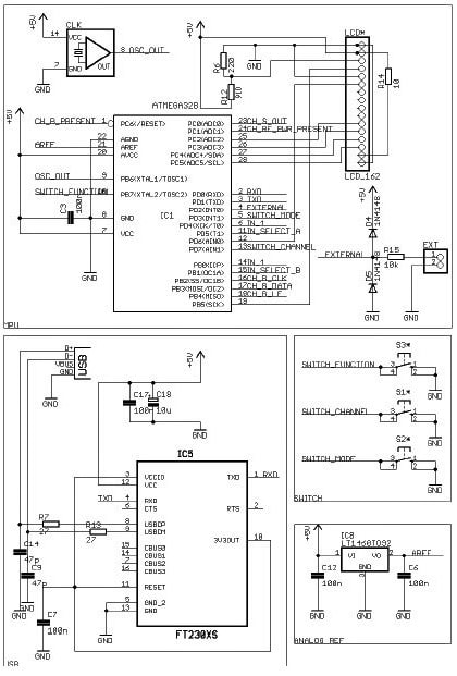
Figure 2 : Schematic Part 1
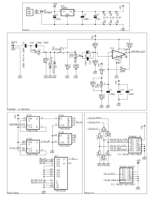
Figure 3 : Schematic Part 2