At The Repair Bench
Chris Prioli, AD2CS
A Monthly Column Describing A Recent Repair Bench Event
WWW.AD2CS.COM

|

|
Para Dynamics PDC-50DL Dummy Load - August 2024
|
It never ceases to amaze me that people will spend good money to repair equipment that is less expensive to replace than it is to repair. That was the case with the Para Dynamics PDC-50DL fifty-ohm one-hundred-watt dummy load that showed up at my door.
|

|
The complaint was that the owner smelled a “burnt electronics” odor from the dummy load, and when he measured the through-resistance of the load, it was no longer 50.1 ohms as it had been. Instead, it was closer to 54 ohms, and he wanted the unit repaired.
When I put it on the bench, the first thing that I did was to measure the through-resistance of the load, which came in at 53.8 ohms. Now this is clearly not fifty ohms as the load was labeled, but it was not terribly far from it. I decided to open it up and see what was what inside the unit.
When I put it on the bench, the first thing that I did was to measure the through-resistance of the load, which came in at 53.8 ohms. Now this is clearly not fifty ohms as the load was labeled, but it was not terribly far from it. I decided to open it up and see what was what inside the unit.

Charred Spot On PCB
|

PCB With Resistors Removed
|
Upon removal of the cover, I discovered that the architecture of the unit was a set of forty-eight 270-ohm 2W resistors configured as sixteen parallel sets of three resistors each, with each group of three resistors set up as individual series strings. Thus, we had 16 parallel resistances of 810 ohms each. Some simple mathematics shows that the total resistance would be 50.625 ohms (810 divided by 16). However, the resistors were 5% types, meaning that each series string could have been anywhere from 769.5 ohms to 850.5 ohms. Taken at the high end, and assuming all were the same, we would now have 850.5 divided by 16, or a potential high resistance of 53.15625 ohms. I wondered just what his concern was until I looked at the other side of the PCB sandwich that comprised the body of the dummy load. There, it was obvious that a resistor had gotten very hot, as the board was charred.
I attacked the unit with the soldering iron, first removing the dummy load body from its enclosure, and then removing the three resistors in the series string that was centered at the charred spot. What I found was that all three of these resistors had failed catastrophically, and that that particular series string was in fact not in circuit at all, but was fully open.
I attacked the unit with the soldering iron, first removing the dummy load body from its enclosure, and then removing the three resistors in the series string that was centered at the charred spot. What I found was that all three of these resistors had failed catastrophically, and that that particular series string was in fact not in circuit at all, but was fully open.

Resistors Replaced (Opposite PCB)
I had the same type and value resistors in stock, so it was a simple job to install three new resistors at that location in the array. I did so, and then I reassembled the dummy load. Now when measured with the ohmmeter, the resistance showed as 50.1 ohms from the SO-239 center pin to the body of the dummy load.
So… why did these three resistors fail, and why did they fail in the manner in which they did? I cannot answer that with any degree of certainty. I can make the assumption, however, that excessive power was input into the load and that this failure was the result. Maybe they were the “weak link” in the resistor chain. Maybe the soldering at those resistors was poor and heat developed as a result. “Maybe” is a big and powerful word, because it can mean so much and so little at the same time. All that I know for sure is that the dummy load is now back to its nominal fifty-ohm value, though in reality it was never very far off from that value, and was just barely outside of the tolerance range for the components used in its construction. Finally, I would like to mention that the 100-watt rating is a bit hopeful, as on its best day, two watts each at forty-eight resistors only provides for sinking 96 watts. What a slippery slope.
See you next month.
MFJ-941E Versa Tuner II - July 2024

A short while ago, one of our fellow GCARC Club members asked me about making a repair to his MFJ antenna tuner, a model 941E Versa Tuner II (Figure 1). It seems that he had grown tired of having to shine a flashlight on the panel meter to read the crossed needles at night. Apparently, the factory illumination for the panel meter, a 12V incandescent lamp, had failed, as they are prone to doing. I decided to make a far more permanent repair by fitting a white LED in place of the incandescent lamp. I also noted that one of the four rubber bumper “feet” for the unit was missing.
I opened up the unit - a total of eight screws, with three on each side and two across the top front of the cover - and checked to make sure that the lamp had actually failed and that there was not some other problem. With 13.8V supplied to the rear panel power inlet for the lamp, and with the lamp switch in its “ON” position, I had the full 13.8V across the (dead) lamp. Lamp failure was confirmed.
I opened up the unit - a total of eight screws, with three on each side and two across the top front of the cover - and checked to make sure that the lamp had actually failed and that there was not some other problem. With 13.8V supplied to the rear panel power inlet for the lamp, and with the lamp switch in its “ON” position, I had the full 13.8V across the (dead) lamp. Lamp failure was confirmed.
|
I removed the lamp holder from its place in the meter housing (Figure 2), and then set about removing the lamp from the holder. That took a little bit of doing because of the manner in which the lamp’s bare wire leads had been fed through the holder and wrapped around the socket terminals of the holder. In addition, there is a 0.01µF ceramic disc capacitor across the lamp, and that had to be dealt with as well. I worked at it, and eventually had the holder completely stripped and disassembled.
|

Figure 2 : Lamp Holder In Meter Housing
|
Disassembly of the holder was necessary in order to make a provision for the LED leads to pass through the holder base alongside the socket terminals. The LED leads are much heavier than were the lamp wire leads, and I needed to make holes for the leads to run through. That was simple enough, using a “T” pin and a pair of long-nose pliers to push the pin through the plastic alongside the terminal contacts.
I gathered up the necessary parts - a white 5mm LED, a 510Ω 250mW 5% resistor for current limiting, and a replacement for the 0.01µF capacitor that was unavoidably damaged in removal. The LED fit perfectly into the lamp holder, and I wrapped the LED leads around the terminal contacts. I then added the resistor to the cathode terminal, after which I installed the capacitor across the LED.
I soldered the components in place and formed a small hook on the opposite end of the resistor, so as to facilitate connection of the cathode lead there. Finally, I soldered the lamp circuit wires to the lamp holder terminal (anode) and to the resistor (cathode), cleaning up the excess lead lengths.
|
The incandescent lamp and the LED emit light in different patterns. The incandescent lamp emits its light in a diffuse pattern all around the lamp envelope without any particular focus. The LED, on the other hand, emits most of its light in the forward direction off the end of the LED envelope. This caused an objectionable “white spot” to appear in the center of the meter when the LED was powered up. I resolved that issue by applying a dome cap of copper tape (Figure 3) to the very end of the LED envelope, blocking most if not all of the light in the immediate forward direction. As a result, the
|

Figure 3 : Copper Tape On End Of LED
|
illumination of the meter is now more diffuse while still being sufficiently bright for reading the meter under any ambient light level. I installed the cover and gave the unit a final look-over.
At that point, I remembered the missing rubber bumper “foot” on the unit. I removed the remaining three bumpers, which were barely holding on, and cleaned the surface thoroughly with some 99.9% IPA. Then, I installed a matched set of four new bumpers to the bottom of the unit. Job done.
Sometimes, repairs can make a piece of equipment better than the factory design level. I am not sure, in today’s electronic world, why MFJ chose to use incandescent illumination other than maybe the fact that it made diffusion of the produced light a non-issue and therefore cut some minor expense. However, it also built in some planned failures, which could easily have been avoided. This unit should never suffer another panel meter illumination failure.
See you next month!
Icom IC-756 PRO Transceiver - June 2024
|
One of my fellow GCARC members called me one day because he was having some difficulties with his Icom IC-756 PRO (Figure 1), particularly in tuning the set via the VFO. While I helped him to determine that his biggest problem was the fact that the VFO was locked, I could not account for all of the behavior of the radio. He asked me to put it on the bench and give it a good once-over. |

Figure 1 : Icom IC-756 PRO
|
I found that almost everything was normal with the set, with one glaring exception. The VFO worked very intermittently. It the dial was turned very slowly, it would tune, but it would skip for one half of the revolution of the VFO knob. If the knob was spun rapidly, it would not tune at all.
A quick look at the IC-756 PRO schematic showed that the VFO utilizes a magnetic encoder as its control device. Removal of the front panel, and partial disassembly of that panel, was necessary to access the encoder in its installed location. I quickly determined that the encoder has suffered some sort of a mechanical failure in that a black powdery substance was coming out of the encoder body along the encoder shaft. I attempted a cleaning of the encoder, but to no avail. The encoder still behaved badly, so I determined that a replacement encoder was required.
A quick look at the IC-756 PRO schematic showed that the VFO utilizes a magnetic encoder as its control device. Removal of the front panel, and partial disassembly of that panel, was necessary to access the encoder in its installed location. I quickly determined that the encoder has suffered some sort of a mechanical failure in that a black powdery substance was coming out of the encoder body along the encoder shaft. I attempted a cleaning of the encoder, but to no avail. The encoder still behaved badly, so I determined that a replacement encoder was required.
|
The encoder (Figure 2) has a part number on it (RMS20-250-201P), which turned out to be a Nidec magnetic encoder having 250 pulses per revolution and designed for operation on 5VDC, with “A” and “B” square wave outputs in quadrature. I ordered in a replacement encoder from one of my standard suppliers, knowing that the received encoder would not have the four-pin plug on it, being terminated as wire leads instead. It took only a couple of days to receive that encoder, but when it came in, I discovered that the encoder used by Icom in this case, while carrying that part number, was in fact a custom variation of that part, having a shaft that is approximately 15mm longer than the shaft on the standard part. Obviously, this encoder was not going to fit properly in the radio, in that the shaft would not extend far enough through the front panel for the knob to mount on it properly. |

Figure 2 : Icom IC-756 PRO Encoder
|
I ended up locating another encoder, this one having the correct length shaft and the pre-installed four-pin plug. It carried an Icom part number of 6910011090. I was fortunate in being able to obtain this part at a price somewhat reduced from the normal Icom asking price for the part, which was quite expensive.
When the Icom encoder came in, I installed it and tested the operation of the radio. All worked as it was intended to, and the tuning was, of course, back on track. I put the radio through its paces with the full array of test equipment connected, and all was well. The radio was ready to go back to its owner.
When the Icom encoder came in, I installed it and tested the operation of the radio. All worked as it was intended to, and the tuning was, of course, back on track. I put the radio through its paces with the full array of test equipment connected, and all was well. The radio was ready to go back to its owner.
The lesson learned in this repair is that even when a part carries a part number that matches up with a manufacturer’s standard parts offerings, it may still be a customized and therefore a proprietary part. This makes sourcing a replacement part somewhat more difficult, and can severely limit the cost-savings effect of purchasing a standard off-the-shelf part for a repair.
|
As a final point, I had done some research into Icom IC-756-series encoder (Figure 3) issues and I found that this is a quite common failure, in most cases with the encoder going out of alignment or failing due to the failure of one or both halves of the dual comparator IC that is integrated into the encoder assembly. There is information on the web about repairing these encoders from a realignment standpoint and also from a replacement of the IC standpoint. It turns out that an ubiquitous LM393 dual comparator IC in its SMT form factor will do the job nicely. |
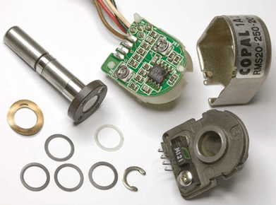
Figure 3 : Icom IC-756 Encoder Fully Disassembled
|
The reason that I opted for replacement of the encoder is two-fold : (1) while the price of the LM393 comparator is minute, the time that it takes to disassemble the encoder and replace the IC would cost the owner more than the cost of the replacement encoder, and (2) the fact that the black powdery substance was coming out of the encoder tells me that there was physical damage internal to the encoder as well as whatever electronic damage existed.
Had the radio been my own radio, I may have experimented with repairing the encoder. With the radio belonging to a customer, I chose to err on the side of caution, as I would have to stand behind my work. Oh yeah - one other thing. There is also a case documented online about a ham who used one of the standard encoders in an Icom IC-756 and extended the shaft length via the use of a coupling collar and a cut-off shaft from a potentiometer. It turns out that as an idea, that is not half bad. The problem is that there is not much room for any kind of standard 1/4" coupler to fit in there, so instead, I have discussed having custom single-piece extenders turned from aluminum rods. I have provided a fellow GCARC member with a drawing of what I would like the extender to look like, and as of this writing, he has made a small quantity of these shaft extenders for my use. I have also had a few shaft extenders manufactured for me via the 3-D print process. As it turns out, I have now installed both types of shaft extenders. When the metallic type is installed, I have found it advantageous to also install a copper leaf spring contact that maintains a positive connection to the knob and shaft, and which is connected to the radio chassis. This provides an effective ground path for the static electricity that may find its way onto the shaft from the operator’s touch.
It also turns out that Icom uses the same encoder with the standard (shorter) shaft in other radio models, including the IC-718, where it seems to see frequent failures, presumably due to static discharge through the encoder knob and circuit to ground. I will hang onto the standard encoder, as it will probably find a use at some point in the future.
See you next month!
Yaesu FTM-400XDR Transceiver - May 2024
|
Sometimes, a repair does not only involve schematics, components, and solder. That was the case recently when a Yaesu FTM-400XDR (Figure 1) came in for repair. The FTM-400XDR is a dual-band 2m/70cm mobile radio with digital, data, APRS, and Bluetooth capability in addition to the usual analog modes.
The radio’s owner brought it to me, saying that it would not allow him to reach the Club’s repeater at 147.180 MHz. He and I, several weeks prior, had spent some time noodling |

|
around with the radio for the same complaint, and I found then that it worked quite well in simplex mode, and that when I entered the correct CTCSS frequency and set the radio for automatic repeater offset operation and proper squelch mode, it worked well on the repeater as well. I told him to go through the programming of the radio and at that point I believed that the problem was resolved.
Fast-forward a few weeks, and the radio is back, this time having been replaced by an FTM-500 series unit out of frustration (and probably a little bit of desire). The more features any given radio offers, the more complex the operation and therefore the setup or programming of that radio will be. This is what turned out to be at the root of this failure, but I am getting ahead of myself.
Having the previous history in mind, the first thing that I looked at was the programming of the memories in the radio. What I found surprised me. There were no stations programmed other than the Club’s 2-meter repeater, and that one had an incorrect CTCSS frequency entered. The tone was set to 100.0 Hz rather than to the correct 131.8 Hz. Further, I found that the Squelch Mode setting was set to Noise rather than to either Tone or Tone Squelch. This meant that that the radio was generating a 100 Hz sub audible noise signal instead of the clear 131.8 Hz sub audible sine wave tone required to allow access to the repeater.
Funny thing… I remembered additional memory channels having been populated when I looked at the radio previously. I couldn’t see the owner deleting all of the other channels, including the “Home” channels, so I began to wonder about the memory of the radio. I programmed in three each VHF and UHF repeaters manually, and then I set the radio aside for a few days. When I came back to the radio, the memory slots were not empty, but neither were the stored values the same as I had entered. For example, the text strings assigned to the memory slots had been corrupted, and the CTCSS tone frequencies had changed. In addition, the Squelch Mode settings for each of the memory slots had also reverted to Noise. At that point, I believed that I had narrowed the problem down to a failed memory battery in the radio. This is reinforced by the fact that the date and time stored in the radio, which I had reset, were also incorrect.
Investigation of the radio service manual showed that the radio actually uses two batteries, which are actually coin cells - one each in the Front Panel Module (Figure 2) and the Main Module (Figure 3). In both locations, the cell is an industry standard ML614R-TT31 cell carrying a Yaesu replacement part number of Q9000895. This is a lithium-ion secondary cell with a 3.0V 2.5mAh rating and an anticipated life of five years, and is designed for a discharge rate of 0.005mA. The specifications for these cells are shown in Figure 4. The specification list for the M614R-TT31 shows that it was designed for only a 10% discharge depth, with a charge/discharge cycle count of around 300 cycles.

Figure 2 : Front Panel Coin Cell Location
|

Figure 3 : Main Module Coin Cell Location
|
|
According to the serial number of the radio at hand, it was produced in September of 2020. Making the coin cells almost three years of age in use, but there is no real way of knowing how much of their shelf lives had expired at the time of installation. It is not unreasonable to find these cells to be failing at three years of radio life. Upon opening the radio’s Main module and measuring the mainboard cell, I found it to be at 2.58V. Next, I opened up the Front Panel module and measured that cell. The Front Panel module cell measured out at a very low 0.612V. It was obvious at this point that replacement of both of the cells was necessary, so I ordered them in. As it turned out, even though the FTM-400 uses two of these cells, Yaesu’s USA service center Standard Horizon stocks only one of these cells. They get $1.49 for each cell and about $11.00 for the shipping, and said that the second cell would have to come from Asia and would entail additional shipping charges. Instead, I ordered a set of ten cells from an Asian supplier at a reasonable cost and with less than a two-dollar shipping fee. The only rub is that the cells, ordered in the middle of May, are not projected |

Figure 4 : Coin Cell Specifications (ML614R-TT31 Boxed In Red)
|
to arrive until almost the end of July, about the same lead time that Yaesu had offered.
You would think that a consumable item with a finite life cycle such as these lithium-ion cells, which also have a relatively low expected charge/discharge cycle count before failure, would be more readily available here, where so many of these radios have been sold. The Yaesu parts counterman said that he only gets orders for these cells one at a time. That may well be, as other models use the same cell but in a single cell scheme. The FTM-400, however, uses two of these cells, and the manufacturer should be ready to support the radios as these cells fail. The failure of these cells is inevitable and should therefore be anticipated, with an accompanying adjustment in stocking levels. This looks like poor planning, if you ask me.
OK - the batteries - or cells, to be more accurate - have arrived and have been installed. Now the voltages measured are as follows: 2.98V on the mainboard, and 3.02V on the front panel board. Hopefully, this repair will keep the memories in this radio operational for several years. These cells are lithium-ion secondary cells, which are rechargeable, and they do receive a charging current during radio operation. However, there is a finite limit to the number of discharge/charge cycles which the battery can experience before it will fail to accept additional charging. It is safe to assume that between the relatively short “shelf” life and the limited “cycle” life of these cells, they have simply met their limits and needed replacement.
Replacement of the cells was straight-forward. I used my SMT soldering tweezer to heat both tabs of each original cell at the same time, simply lifting the cell clear once the solder flowed. The soldering tweezer was not used to install the new cell, as I did not want to place a short across a new cell. I simply placed each cell into its proper position onto the pre-tinned pads on its respective board, and then soldered it in place with my pencil iron. To simplify the installation, I pre-tinned the solder tabs and the PCB pads before placing the cells on their boards. Having done that, the final step was a simple reflow of the tinning solder.
Following the installation of the cells, it was time for the radio to be programmed and tested. I used the RT software and cable provided by the radio owner for the programming steps. Once that was completed, I took the radio to an antenna, feeding the output through my trusty Bird 43 directional wattmeter with an appropriate element in place.
All operational testing of the radio went as expected. The output power level on the 2-meter band measured a nice 49.2 watts on the High Power setting, 19 watts on the Medium Power setting, and 4.75 watts on the Low Power setting. The 70-centimeter band did not fare quite as well, measuring 46.5 watts on the High Power setting, 18.25 watts on the Medium Power setting, and 4.5 watts on the Low Power setting. While all of these power levels are somewhat lower than the advertised maximums for this radio, they are none the less within reasonable limits for each of the individual power level settings, and were therefore accepted as being “normal”.
It must be noted that Yaesu does not publish an output power range for each band in their service manual for this radio, choosing instead to publish only the maximum power levels expected. The technician must then make a decision as to whether or not a given measured output is acceptable. I considered 10% to be a reasonable lower limit for the various power levels, therefore giving us lower limits of 45 watts, 18 watts, and 4.5 watts respectively for the three power levels offered in this model - high, medium, and low. All of the power measurements were either above or right at these lower-level limits, and were therefore accepted as being within “normal” operating power ranges.
All that was left now was to reassemble the radio, do a final after-reassembly test, back up the programming to the onboard micro-SD card, and get the radio back to its owner. As a convenience to the owner, I printed off a copy of the service manual, so that he would have one for any future needs.
In summary, it can safely be said that this family of radios is coming of age to the point where they will begin requiring lithium-ion cell replacements, as these cells are about at the anticipated extent of their life spans. This means that more of these radios will be coming in for coin cell swaps, and the repair shops should be prepared to service these units. I have now got sufficient inventory on these cells and I am therefore quite prepared. I hope that other repair facilities follow suit and get themselves ready for the rush, as quite a lot of these radios have been sold.
See you next month!
Conar Model 231 Tuned Signal Tracer - April 2024
|
Back in August of 2023, a customer asked me for some help in making his late 1970’s-vintage Conar Model 231 Tuned Signal Tracer (Figure 1) operational for him. A little bit of history is called for here. Conar Instruments was the electronic equipment division of National Radio Institute (NRI). National Radio Institute - McGraw Hill Continuing Education Center was a private, postsecondary, for-profit correspondence school based in Washington
DC, from 1914 to 2002. NRI launched the Conar division in the fall of 1961 and began selling test equipment (and other items) to |

|
their students primarily in kit form in early 1962, some of which were assembled as a part of the home study program. Other items were simply made available for purchase, assembly, and use by the students in their new electronics repair trade. The Conar 231 Tuned Signal Tracer was released around 1978, and several hundred were sold.
The 231 is an easy-to-use, all solid-state tuned signal tracer. It is called a tuned signal tracer because it has three selectable ceramic filter controlled tuned inputs covering the standard broadcast IF frequencies of 262kHz, 455kHz, and 10.7MHz. These tuned circuits eliminate the need for manual tuning as was required when using some other signal tracing units. This design simplifies the operating setup, allowing the technician to spend his or her work time where it counts - locating and repairing the defect. The Model 231 also provides two untuned input selections, an RF option and an AUDIO option. The unit schematic is shown in Figure 2. This schematic was derived from the unit itself and was drawn in the ExpressSchematic software that I like to use.
The 231 is an easy-to-use, all solid-state tuned signal tracer. It is called a tuned signal tracer because it has three selectable ceramic filter controlled tuned inputs covering the standard broadcast IF frequencies of 262kHz, 455kHz, and 10.7MHz. These tuned circuits eliminate the need for manual tuning as was required when using some other signal tracing units. This design simplifies the operating setup, allowing the technician to spend his or her work time where it counts - locating and repairing the defect. The Model 231 also provides two untuned input selections, an RF option and an AUDIO option. The unit schematic is shown in Figure 2. This schematic was derived from the unit itself and was drawn in the ExpressSchematic software that I like to use.

Figure 2 : Conar 231 Schematic Diagram
The unit came in to my shop as an inoperative piece of equipment that was also missing its test probe and ground connector. Those two items are actually the subject of one of my build articles previously published at this point, as I designed and built a replacement active amplifying probe with the high input impedance necessary to avoid loading of the circuit under test and therefore obtaining undistorted waveform samples. The subject of this article is the actual repair of the Conar 231 main unit.
|
This model is powered by 117VAC line current into a step-down transformer with a center-tapped secondary, which then produces two operating voltages, a +15VDC source and a +12VDC source (Figure 3). The +15VDC is taken directly off the rectified and filtered output of the power transformer, while the +12VDC output is tapped off the full wave rectifier and regulated down to twelve volts via a 2N2124 transistor and a 1N5242B 12V Zener diode. The +15VDC source is filtered by capacitor C220, a 1000µF/25V axial aluminum electrolytic capacitor, and the +12VDC
source is further filtered by capacitor C221, a 330µF/16V radial aluminum electrolytic capacitor. |

Figure 3 : Power Supply Section
|
On power-up, the +15VDC supply was found to be varying from about +6VDC up to about +19VDC, most likely as a result of heavy ripple imposed upon the source. The only possible cause of this ripple was the 1000µF filter capacitor C220. At the same time, the +12VDC supply was found to be dead. As a starting point, I removed and tested capacitor C220 and also C221 (the 330µF filter for the +12VDC source). The 1000µF capacitor turned out to be extremely leaky, while the 330µF capacitor was shorted. I replaced these two capacitors and went back to my testing routine. Now the +15VDC source was as it should have been, but the +12VDC supply was still dead. Voltage measurements at the 2N4124 pass transistor Q201 showed that the transistor was shorted, as was the 1N5242B 12V Zener diode. Replacement of both of these components restored the +12VDC source to proper operation.
At this point, I thought that I had the problems solved, but it turned out that there was still another problem. In testing the operation of the signal tracer, I found that there was no audio from the speaker at all, and no activity at all on the front panel signal strength meter. It was obviously time for some more tests to be made.

Figure 4 : Audio Amplifier And Output Section
I fired up my signal generator and set it for a 1kHz sine wave output at about a half of a volt amplitude. I then injected that signal at the input of the LM380 audio amplifier, IC103 (Figure 4). There was no signal throughput to the speaker at this point. I checked all of the IC voltage readings and they were all right on the money, where they were supposed to be. That led me to the most likely culprit being C218, a 1µF/35V tantalum capacitor in a shunt position across the speaker. I removed and tested that capacitor and found it to be shorted. Replacement of the tantalum capacitor restored the audio operation to normal.
With three failed polarized capacitors in this unit so far, and considering the age of the unit and therefore its capacitors, I elected to go proactive and replace the remaining polarized capacitors, which included a pair of 100µF/25V axial electrolytics, a second 330µF/16V radial electrolytic, and a single 220µF/35V radial electrolytic. It was good repair practice to replace all of these capacitors based upon the rate of failure already seen and the overall age of the parts involved.
This is a fairly well-designed signal tracer, and in spite of the screwy component numbering scheme used, it is not at all difficult to work on. The single PCB is retained in a modular fashion to the chassis by a set of four nylon retaining stand-offs, setting down onto a pair of ten-position pin connecter strips. The PCB itself has receiver sockets that mate with the pins in the connector strips.
As a footnote, one of the things that I noticed was that the red paint had all come off the needle of the front panel signal strength meter, and was sitting in pieces on the floor of the meter shell. I removed and disassembled the meter, cleaning out the paint particles. I then masked the meter face and re-painted the needle with some red color. After re-assembly, it looked as good as new.
All in all, a fairly easy repair, though there were multiple failures to be tracked down and corrected. The moral of this story is that it’s not done until it is all done. I packed the unit up together with the new probe and ground lead that I had fabricated, and shipped it back to its owner.
See you next month!
Heathkit® IT-5283 Signal Tracer - March 2024
|
As is well-known by now, I have a tendency to take on unusual projects, especially those that others cannot seem to repair. This was the case recently with a Heathkit® IT-5283 Signal Tracer (Figure 1) that came in for repair. It was shipped to me in “inoperative” condition, with no other information except that the owner purchased it on ebay.com and was disappointed when he was not able to get it to work at all. He is a hobbyist, but is not much of a repair technician, though he did say that he took voltage measurements with a fresh pair of batteries, but could not find any operating voltages anywhere on the main (and only) circuit board. |

Figure 1 : Heathkit® IT-5283 Signal Tracer
|
The IT-5283 is one of a five-piece test equipment family of about an early- to mid-1970’s vintage. The family includes a multimeter, an audio signal generator, an RF signal generator, an RLC bridge, and this signal tracer. All five units share a common design as regards form factor and appearance, residing in two-piece plastic enclosures. The kit builder had the option of powering the units either from a pair of nine-volt snap-top batteries, or from a specialized five-output power supply that offered ±9VDC to each of its five output cables. The power supply, Heathkit® model IPA-5280-1, is very hard to come by today, but it is not very hard to duplicate. Each of the five output cables was terminated with a Molex® three-pin 0.093” connector. If the kit builder chose to power the kit from the power supply, there were five sets of parts that came with the power supply kit and that were used to modify each of the 5200-series test units to accept power from the power supply. I mention all of this because it is an important point in the repair of this unit.
When the power supply conversion was made to the test equipment, regardless of which specific model it was, a removable blocking panel gets taken out of the back of the enclosure, and a replacement panel got installed in its place. The new panel (Figure 2) held a slide switch used to select between battery power (for portability) and the line power from the power supply. In addition, this panel also held the mating Molex® three-pin connector so that the power supply cable could be tied in to the unit. OK - more about this later… just remember this detail.
When I received this unit for repair, there were no batteries installed, so I put a fresh set of nine- volt batteries into the snap connectors, got out the voltmeter and my signal generator, and set out to test the unit. I set the signal generator for a one-volt peak-to-peak signal at one kilohertz, connected its output to the signal tracer input, and turned it on. Needless to say, there was nothing - not even static or noise - from the signal tracer. So far, my findings matched what the owner told me - no operation.
I opened up the housing to access the circuit board, and got out a schematic of the unit (Figure 3) from my Heathkit® library, and started to check for voltages on the printed circuit board (PCB). Once again, the owner was correct in that there was absolutely nothing alive on the PCB. Knowing that I had a pair of good batteries, I went to the power switch, which is a section of the rotary function selector switch on the front panel. The switch was badly oxidized, so I cleaned it up with some DeoxIT®, but that was not the problem, as I was not even getting power to the switch. The only thing between the batteries and the power switches (there are actually two power switch sections in the selector switch, one for +9VDC and one for -9VDC) is the PCB, the power source selector switch on the back panel, and the wiring between them. A quick look at the power source selector slide switch showed that it was installed (or wired) backwards, so that the “BATTERY” position was actually indexed to the “LINE” indication on the panel. A simple fix for this one, I thought. Simply dismount the switch, rotate it 180°, and remount it. Once I saw that problem, I simply moved the switch to the correct position (I would turn it around later) and continued with my testing.
When the power switch was turned on, I now had power to the PCB at both voltage levels as appropriate for the function selector switch position. However, as I quickly discovered when I powered up the signal generator again, there was still no output at all from the signal tracer speaker - not even static or noise - the same as earlier.
I started probing the PCB (Figure 4) for actual voltages in accordance with the schematic, and I quickly found that the operating voltages for transistors Q6, Q7, and Q8 were very low, with no voltage present at all on Q8. According to the schematic, there is a 250µF electrolytic capacitor (C11) that is connected to the collectors of Q6 and Q7, and if shorted or very leaky, would drag those terminals, and by extension Q8, right down to low levels. I removed that capacitor and tested it. It turned out to be extremely leaky, testing out more like a 98Ω resistor than like a capacitor. I replaced it with a 220µF 25V electrolytic from my inventory, and the unit came alive.
I was not finished there, however, as although it was alive, it was extremely noisy when the level (gain) potentiometer was rotated, and from time to time there was a loud “pop” in the speaker as well. Some more investigation turned up another failed capacitor, this one a 10µF electrolytic in the level control circuit. I replaced it with a like 10µF 16V electrolytic capacitor from my inventory, and the “pop” was gone. Some DeoxIT® spray took care of the noisy level potentiometer as well.
With two of the seven electrolytic capacitors in this unit having failed, I opted to replace all of the electrolytics, three (total) 250µF (replaced by 220µF), two 50µF (replaced by 47µF), and two (total) 10µF capacitors. Once that was completed, I went over the rest of the unit to check for any other problems, and I found one wire in the “LINE” power circuit that was not soldered to the PCB. It was in the hole in the PCB, and because it was solid rather than stranded wire, it stayed in place, but the circuit would have been problematic at best, if it worked at all. Of course, I soldered this wire in place properly. I then remounted the power source selector switch in its proper orientation, gave the unit a good cleaning, and buttoned it up. Finished!
Truth be told, I have to wonder if the original builder of this unit ever got it to work at all, or if the builder just never noticed that the power source selector switch was backwards. While that individual may have known and not cared that it was backwards, that little problem sure caused some grief for at least one later owner of the unit. It is a safe bet that the current owner never noticed the backwards switch, as he was lost as to why there was no incoming supply voltage to the PCB.
It takes a systematic approach to any problem if you want to find a solution to the problem. It certainly does not pay to just go jumping from place to place, and guessing or assuming anything. Know what you have, and know what you expect to find. Then, when you don’t find what you expected to find, look for the reason why the result is different. With a logical and systematic approach, you will find the answer.
See you next month!
LF&C Survey Meter - February 2024
Not long ago, I wrote in this column about a geiger counter repair that I was asked to take on. As you may (or may not) recall, I wrote at that time that the Club member for whom I was making these repairs actually brought two “geiger counters” in for repair. The previous article described the operation and repair of a Victoreen CD V-700 Model 6A Radiological Survey Meter. Now, I am telling the rest of the story, as Paul Harvey used to say. This month, I am describing the operation of and repairs to a Landers, Frary & Clark CD V-715 Model 1A Radiological Survey Meter (Figure 1).
As I explained in the previous article, these geiger counters and radiological survey meters were manufactured under the auspices of the federal Civil Defense program, each being made to a specific standard for its CD type designation, but with the specific circuitry and operational design left up to the individual manufacturers of the equipment. Thus, there were several different makers of the CD type V-715 meter. Landers, Frary & Clark (LF&C) was just one of those manufacturers.
While the V-700 meter described in the earlier article is a geiger tube instrument, the V-715 utilizes an ionization chamber as the sensing element instead of a geiger tube. As a result, the V-715 is not really a “geiger counter”, though that term has been loosely used to describe meters of this type as well.
One thing that sets this type of instrument apart from the others is that it uses some resistors having extremely high through resistances. Connected to the range switch in this unit (refer to Figure 2 and Figure 4) are resistors having the following values, all of which are specified as 500mW 20% metal film types as below :
- 2 pieces, series connected, of 1 x 10¹¹ ohms (100,000,000,000Ω) each;
- 1 piece of 2 x 10¹⁰ ohms (20,000,000,000Ω);
- 1 piece of 2 x 10⁹ ohms (2,000,000,000Ω); and
- 1 piece of 2 x 10⁸ ohms (200,000,000Ω).
The lowest of these values is 200 megohms, well above the capability of most ohmmeters to measure. This poses a bit of a problem when attempting to validate the condition of such a resistor. One method of determining the resistance would be to apply a fixed voltage source to the resistor and then to measure the current flowing through it. But, at 200 megohms, a testing voltage of 100V will cause only 500 nanoamperes (0.0000005A) to flow - well below the measurement range of most typical ammeters. So… how is the resistance measured? One method that often works is to first isolate the resistor under test, and then to place a resistor of known value in parallel with the resistor under test. Measure the parallel resistance and work the arithmetic backwards to determine the value of the resistor under test. However, even this method is not useful in this circumstance due to the sheer magnitude of the resistances of the resistors to be tested. Placing a 1MΩ 0.1% tolerance resistor in parallel with the smallest of these high-value resistors, the 200,000,000Ω one, gave me a measured resistance of 994,130Ω. This value is outside the tolerance range of the 1MΩ 0.1% resistor (100,100,000Ω to 999,000Ω), but would be a resultant value that is well within the tolerance range of the 200,000,000Ω 20% resistor (240,000,000Ω to 160,000,000Ω) and 1MΩ resistor placed in parallel, so the arithmetic would be meaningless in determining the actual value of the high-value resistor. It should be noted that the 994,130Ω reading obtained is pretty close to what would be expected with a 200MΩ and a 1MΩ resistor of close tolerances in parallel with each other - (200,000,000 x 1,000,000) / (200,000,000 + 1,000,000) = 995,025Ω.
My everyday RLC bridge is capable of only 10 megohms, while my HP4284A laboratory RLC bridge tops out at 99.99 megohms in its resistance mode, well beneath the lowest value used in the range selector section of this unit. I decided that I could not measure these resistors by any practical method, so I would have to assume that they were acceptable until some operating condition of the unit showed me otherwise. In reality, based upon the resistor types in place and the age of the unit, I would have to believe that these resistors were replaced at some point in the history of this unit, which belief is reinforced by the fact that one range position (the x 0.1 position) that called for two series resistors now has a single wire-wound tubular glass device instead.
OK - on to the general description of the unit. This meter is powered by a single standard “D” cell at 1.5VDC, but generates a maximum potential of -60V from the secondary of the power transformer. The primary of that transformer is in the oscillator circuit, which includes a GI 1459 PNP germanium transistor (more about this later).
As mentioned previously, the sensing element is a hermetically sealed plated steel ionization chamber. This chamber (Figure 3) consists of a shell and an insulated center electrode called a collector, which is mounted to a high-resistance insulated feed-through connector. A strong voltage potential is applied to the collector and ionization chamber shell, which makes the shell (with respect to electrical common) negative by about a sixty-volt differential. This negative charge attracts the positively-charged ions that are formed by gamma radiation passing through the air that is contained within the ionization chamber. The ions striking the ionization chamber shell cause a current to flow in the collector. This current is proportional to the number of ions striking the shell, and therefore proportional to the strength of the radiation field. What appears to be a date (June of 2011) is penciled on the top of the ionization chamber. It is a possible surmise that this is an historical replacement date for the ionization chamber.
Depending upon which range has been selected by the range selector switch, this very small collector current flows through and develops a measurable voltage across one of the extremely high value resistors discussed earlier and clearly visible, attached to the range switch in the Figure 4 photo. This voltage is applied to the grid of the triode-connected 5886 Electrometer Tube, causing a small current to flow in the grid circuit. To give some idea of just how small this grid current really is, I took a quick look at the Tung-Sol 5886 Pentode Electrometer Vacuum Tube Datasheet. The maximum grid current, in accordance with the datasheet limitations, is 2.5 x 10⁻¹³ amperes when the tube is used as a triode, as it is in this circuit. Written in another form, this current we are talking about measures a mere 0.00000000000025 amperes! The grid current causes a proportional plate current to flow in the tube, with any change in the plate current being shown on the 0-50µA meter movement that is the user’s indication of a detected radiation source.
In this unit, there is a transformer that has a pair of primary windings, one of which has a through resistance of 1.4Ω while the other has a through resistance of 60Ω. The secondary's are also isolated, having through resistances of 890Ω and 85Ω, with the 890Ω secondary paired with the 1.4Ω primary and the 890Ω secondary paired with the 60Ω primary. Used as a step-up transformer, the 1.4Ω primary has a 1:635.7 turns ratio, yielding a very high-voltage output pulse compared to the input pulse voltage in that winding pair.
The remainder of the circuitry uses a handful (seven to be exact) of 500mW resistors of common standard values, easily tested and sourced for replacement, all but one of which are 5% tolerance types. I found one difference between the schematic and parts list and the physical unit, in that R16, a bleeder resistor for capacitor C1, a 5µF electrolytic type, was installed as a 4.7MΩ resistor while the documentation called for R16 to be a of 1MΩ value. Due to the fact that these seven resistors were all of a type - carbon composition - known to exhibit resistance changes over extended time and use, I decided to isolate and measure each of these resistors. In doing so, I found that several of them had varied by well more that their labeled tolerances.
For example, one of the 1KΩ resistors was down to about 400 ohms, while the other was higher than its nominal value, measuring out at 1345 ohms. At 5% tolerance, these resistors should have been no less than 950Ω nor more than 1050Ω. I had all of the required values in stock as modern carbon film 5% tolerance 500mW rated types, so I replaced all of these resistors with new ones, maintaining the 4.7MΩ value as installed for R16.
Next up were the capacitors. Both of the ceramic capacitors tested out as being within specifications and were therefore usable, so they were left in place. The sole electrolytic, on the other hand, had an ESR that was off the top end of the meter scale on my ESR meter, and measured out as about 31.25µF instead of its nominal 5µF as regards capacitance. The top of the ESR meter scale is five ohms, so that capacitor was at least somewhat leaky. It is this leakiness that leads to a higher-than-normal capacitance measurement, as current continues to flow into the capacitor long after it should have stopped if the capacitor had been in good condition. Left alone long enough, that capacitance meter reading would have increased even more - I stopped the test at that point as it was obvious that the capacitor was non-suitable for use. It was replaced with a modern 4.7µF 50V 5% 105°C axial aluminum electrolytic capacitor. Such tight tolerance was not really necessary in this capacitor used as a filtering device, but that is what I had on hand, so I used it. The 4.7µF 50V capacitor is an acceptable replacement for the original 5µF 25V component.
The LC&F meter circuit uses three semiconductor devices - one transistor (mentioned earlier) and two rectifier diodes. The only information provided about the rectifier diodes is that they were “rectifiers”, meaning that they were intended for use in a power supply to convert the AC into DC, and that one had a 50V PIV rating, while the other had a 100V PIV rating. It is unclear why two different diodes were chosen here, as the 100PIV diode should have worked in either location. The original diodes had heavy oxidation on their leads, compromising the lead integrity to the point where they both broke off easily when moved slightly during de-soldering. Through test measurements, I was able to determine that they were both of silicon composition, so I replaced them with a 1N5400 50V PIV 3A diode and a 1N5401 100V PIV 3A diode, both of which were in stock. These rectifier diodes are visible in the Figure 4 photo at the bottom right corner of the PCB.
The transistor was a different story. It was obviously defunct, as it failed each and every test to which I submitted it. I could not make any determinations as to type or specifications from the transistor itself other than the fact that it had gold leads, and its markings were of no help at all. The schematic showed it to be a PNP type. However, what I did find, in the LF&C manual for the unit, was that the original transistor supplier was General Instruments, and that it was a GI part number 1459 device. You might think that having a manufacturer’s name and his part number for the transistor would make it easy to obtain more information about it, right? Not so much, as it turns out. I could not find anything resembling specifications for this transistor anywhere on the internet. I then had a brainstorm and turned to my NTE Electronics QUICKCross™ cross-reference software, where the first item turned up in a text search using “1459” as the search string was the NTE-102 transistor. The datasheet for this device showed it to be a PNP germanium type rated as below :
- Collector-Base Voltage (VCBO)25V
- Continuous Collector Current (IC)150mA
- Collector-Emitter Voltage (VCES)24V
- Emitter Current (IE)100mA
- Emitter-Base Voltage (VEBO)12V
- Total Device Dissipation (PD)150mW
This looked like a good possibility. I mentioned the gold leads because germanium transistors most often have gold leads. I went looking to see who might have stock on this transistor, and I found that Digikey (www.digikey.com) had availability of a direct-ship from NTE with about a five-day lead time. On a whim, I punched “NTE102” into an Amazon search box, and to my surprise, Amazon not only had it, but they had it at about half of the Digikey price. To clinch the deal, the Amazon item order page said that I would have it the next day! What a no-brainer! I ordered it in from Amazon and set everything aside overnight.
OK - so the next day came and with it came the transistor, as promised. Of course, as this point, I really had nothing to go by, that is, nothing saying that this was the correct part other than the NTE cross-reference. On the other hand, I have found the QUICKCross™ software to be quite accurate and reliable with its interchange information. As expected, the leads on the new transistor were in fact gold, and also as expected, based on the datasheet information, was the fact that the transistor was in the same case type, a TO-39 metal can with a tab on its circumference. So far, so good…
Working from the orientation of the original transistor in the PCB and the schematic diagram, the transistor pinout was also correct. The “pinout” is the assignment of specific terminals of the transistor to specific pins on the physical device. In the schematic, the emitter is connected directly to the “D” cell positive terminal. The base is connected to one end of the 1.4Ω transformer primary winding, while the collector is connected to the opposite end of the transformer 60Ω primary winding. Having this connection information, it is easily seen which pin of the original transistor was which terminal of the transistor, which then easily translated to a match with the terminal versus pin assignments of the new transistor. Seeing that everything matched up, I was very confident that I had located a proper replacement for the failed transistor in this unit. I went ahead and installed the new transistor, which can be seen at the lower left area of the PCB in the Figure 4 photo, just to the right of the meter “zero” control potentiometer.
Figure 5 shows a close-up view of the 5886 Pentode Electrometer vacuum tube. I illustrate this tube simply for its curiosity value, as it is somewhat different from those devices that we customarily recognize as vacuum tubes. None the less, it is a vacuum tube. Earlier in this article, reference was made to the fact that the current from the collector of the ionization chamber is directed to both the high-value resistors) via the range selector switch and to the (control) grid of the triode-connected vacuum tube. Note the bare wire lead from the vacuum tube, from the right side of the tube as shown in the Figure 5 photo. This lead ties directly to the common terminal of one deck of the range selector switch, and then also connects directly to the collector lead of the ionization chamber. Note that apart from that one wire, which is soldered, the vacuum tube is connected into the circuit by use of a vacuum tube base socket as are most vacuum tubes. A quick look at the schematic in Figure 2 shows that the cathode is directly heated, and that the cathode is tied directly to the emitter of the transistor.
Once the repairs were made and all operational checks were made in accordance with the manual and the schematic diagram voltage callouts, it was time to button this one up. Field calibration is not really feasible – or even possible in most cases - due to the fact that calibration requires the use of a calibrated radioactive field into which the unit is placed. Then, based upon the strength of the calibrated RA field, the unit is placed into its each of its various operating ranges in turn and each successive calibration potentiometer, one for each range, is adjusted to bring the meter reading into agreement with the known field strength. This requires the use of some equipment not generally available to the field user or maintainer of this device. The manual does indicate which potentiometer is related to which range switch position for actually making the calibration adjustments, but the complete adjustment process requires the use of an X-ray or gamma ray field.
One of the more important factors in the successful operation of this radiological survey meter is the fact that it is sensitive to moisture, including local air humidity. Humidity can and will affect the values of the high-resistance resistors used in the range selection stage as well as the operation of the ionization chamber’s center collector assembly. The high value resistors, the vacuum tube, and the collector assembly are all also subject to problems from handling, as skin oil contamination on the surfaces of these components can cause leakage currents to flow across the component surfaces. When handled, these components must be properly cleaned of all skin oil residue through the use of residue-free alcohol and a soft cloth or cotton swab. To aid in the moisture reduction inside the closed unit, a bag of dry desiccant granules is placed in the bottom of the lower enclosure, which is sealed to the upper body assembly via the use of a rubberized gasket under the cover and O-rings on the control shafts. A rubber cushion is installed in the lower enclosure in the proper location to aid in keeping the “D” cell in its holder. When the unit is assembled, the “D” cell rests on this rubber pad, keeping the cell securely in place.
To close, a few quick words about the manual are actually overdue. I found two different copies of the factory user and maintenance manual for this unit online with a little bit of searching, one more easily readable than the other. The only catch is that care must be taken to ensure that the manual matches the device at hand. Bear in mind that there were multiple manufacturers who produced V-715 radiological survey meters, and each manufacturer may have produced multiple versions of their device. Just make sure that the manual selected is the correct manual for the device at hand, by manufacturer and by specific model number.
All things considered, this was a pretty typical repair of an unusual device. Apart from the fact that the high-value resistors can not easily be measured, the remainder of this repair was pretty straight-forward and required nothing out of the ordinary in either skills or equipment. This was a repair that any reasonably-skilled technician should, be able to handle with ease.
See you next month!
MFJ-259B HF/VHF SWR Analyzer - January 2024
|
I just (at the time of writing this, in early August of 2023) completed the repair of an MFJ-259B SWR Analyzer. The item belongs to one of the GCARC Club members, but had been donated for long-term use to the GCARC Clubhouse. I came across the unit when it was discovered that it would sometimes operate from an AC power adapter, but would not operate at all from its internal battery. What specifically would happen is that the meters came alive, but the LCD panel did not.
The AC power supply for this unit is a 12VDC 1000mA wall-wart type supply. The internal battery is a bank of ten 1.5VDC “AA” cells. The unit is designed to use either regular disposable alkaline cells, or it can use rechargeable Ni-Cad cells. If the Ni-Cad cells are used, a jumper on the MFJ-259B main circuit board must be moved to the “CHARGER ON” position; otherwise, the jumper should remain in the “CHARGER OFF” position. Of course, this is necessary so that the integrated battery charger can recharge the Ni-Cad cells when AC power is provided. |

|
What I found when I opened up the case was a mess. The alkaline cells that had been installed were obviously flat, and had leaked considerably inside the unit. I spent about an hour cleaning the corrosion out of the battery box and the surrounding area. I then replaced the “AA” cells with fresh alkaline cells and tried the unit, to no avail. It would not operate from the battery. Interestingly enough, it also would no longer operate from the external power supply. The same behavior - active meters but dead LCD panel - was exhibited.
This unit was made to the RoHS Directive standard, using lead-free solder throughout. This was evident by the appearance of the solder joints, with their characteristic flat grey appearance so indicative of lead-free solder use. Lead-free solder joints are prone to early failure due to stresses placed on the board and joints, and I also noted several cold joints in various spots on the main board. I went over the board carefully, re-flowing every joint and removing the solder from any that were suspect in appearance. I re-soldered those joints, and again tested the unit. No luck - it was still inoperative in the same manner as before.
This unit has two five-volt DC supplies internally, one of which is used for the oscillator circuit, and the other of which is used for the logic and display circuits. I was getting intermittent five-volt power to the microprocessor and the LCD panel. One of the areas that had cold joints was the power switch on the main board, which is a DPDT latching push-button switch. The two separate sides of this switch provide current to each of the two five-volt supplies. I wanted to validate the power switch, so I removed the switch and tested it out of circuit, where it tested fine. However, after re-installing the switch, the five-volt supply to the microprocessor and the LCD panel came alive. Progress, but not enough. The LCD panel was still dead.
I next took a look at the ground side of the LCD panel. Pin #1 of the LCD harness is the ground wire, while Pin #2 is the +5VDC lead. When I measure the voltage between these two points, I got no voltage reading at all. When I measured Pin #2 to chassis ground, the +5VDC was present. I next placed a temporary jumper wire from Pin #1 of the LCD panel to chassis ground, and the panel came alive and worked normally.
OK - was there an open in the harness to the LCD panel? Or was the problem elsewhere? I moved the jumper wire from the LCD panel to the Pin #1 wire connect point on the main board, and the panel remained operational. This told me that the wire harness was OK, but that the connection point on the main board had lost its ground connection somehow. I re-flowed that joint again, but that still did not solve the problem.
Ultimately, I resolved the issue by soldering in a jumper wire from the Pin #1 connection on the main board to another chassis ground point on the main board. Problem solved.
The mystery still remains as to how and why that particular pad on the PCB lost its connection to the ground plane, but it was not worth digging any further. The intent was to make the unit operational, which I did. The stresses that contribute to the early failure of lead-free solder joints can be thermal stresses, electrical stresses, or physical stresses. It is for this reason that lead-free solder use is prohibited in mission-critical applications like aerospace, military, or medical applications.
What is interesting about this unit, and something that I believe led to the failure of the PCB connection, is the fact that the battery holder for this unit is mounted directly to the PCB, at two points that span the area of the LCD panel connection to the main board. It is likely that the stresses imposed by removing and re-securing the battery compartment caused some flexing of the printed circuit board, resulting in the failure.
Whereas I am not a big proponent of willy-nilly soldering in jumper wires, in this case it was the best solution to the problem at hand. I do not recommend this approach for every open-circuit problem, as there may be another underlying problem that could worsen if not tracked down. In this case, though, I am fairly confident that the problem is related to the lead-free stress failures, possibly internal in the circuit board. So, in this case I used the jumper wire solution to the problem.
See you next month!
Antenna Rotator Controller - December 2023
Back around the end of May, Al KB2AYU came to me and told me that the antenna rotator controller (Figure 1) that I had built and given to the Club for use in the VHF room was “hosed”. A quick look at it showed that he was correct - the display, which should have been showing azimuthal readings between zero degrees and three hundred and sixty degrees, was displaying values way up into the four- and five-digit area (Figure 2), as well as blanking out some of the letters in the word “Azimuth”, which should have been displayed as well.
This controller consists of some very basic parts… (1) an H-bridge motor driver to handle the output current to the rotator motor, including directional (polarity) control, (2) a simple five-volt voltage regulator that drops the incoming 24VDC down to the 5VDC required by the brains of the unit, and (3) an Arduino Mega2560 microprocessor board. A plain Mega2560 shield was built up to bring out the necessary pin connections as well as serve as the PCB for a low-pass filter that is a crucial part of the circuit.
When I say “to bring out the necessary pin connections”, it must be understood that there are many more +5VDC connections and ground connections made back to the Arduino than there are native pins on the Arduino to handle. As a result, a row of eight or nine pins of each type - +5VDC and ground - are set up on the shield. In addition to the LPF already mentioned, the shield also carries the contrast control for the front panel display, which is a blue and white backlit LCD panel with 16 x 2 character capability.
The shield also carries the interface pins for the other controls on the front panel, which include directional motion switches (CW and CCW), preset, park, and speed controls, as well as the bulk of the front panel display connections. This shield board, of course, simply plugs piggy-back style onto the Arduino Mega2560.
I initially thought that maybe a quick reload of the program on the Arduino might solve the problem, in that it may have somehow gotten corrupted. Deciding to try that on the spot, I brought my laptop and a USB-A to USB-B cable into the VHF room, hooked it up to the controller, fired up the Arduino IDE software, and uploaded the program into the Arduino. No joy - the problem remained. I decided then that I would bring the unit home for repair, and I would swap it out with a second controller that I had already built for my own use, but was sitting idle. Originally, I was going to bring the replacement controller to the Clubhouse on Tuesday evening when I went there to teach the General class (Monday was a holiday, and the Technician class was cancelled for that evening). The way things worked out, I was able to bring the fully repaired controller back to the Clubhouse on Tuesday evening instead. Here is what I found…
I began by verifying the operation of the +5VDC voltage regulator, because if that voltage was screwy, the Arduino operation would also be wonky if it worked at all. The five-volt regulator was fine, with a steady output under load of 4.996 volts. No problem there.
Now, as I have already explained in describing the controller, this thing is actually quite simple with a limited number of places for a problem to crop up. Those problems, discounting a wire connection issue, are limited to the voltage regulator, the H-bridge, the display, and the Arduino. The voltage regulator has already been cleared, and the display was evidently operational, as it displayed information - just not the correct information. Simply in an effort to be thorough, I disconnected the plug the carries control signals from the Arduino to the H-bridge, and rebooted the controller, only to find that the same condition existed. Three out of four of the possibilities have now been eliminated, leaving only the Arduino as the culpable component.
Knowing that the programming had already been uploaded to the Arduino once since this problem began, and also knowing that the upload did not resolve the issue, I was left with the base Arduino as the fault source. Now… the Arduino obviously operated, as it was sending data to the H-bridge and the display, even if that data was incorrect. My reasoning told me to try to recover the Arduino and restore its proper operation.
There is a piece of software embedded on the Arduino called the bootloader which basically sets up the operating condition of the Arduino in use. That is the only thing, apart from a possible hardware failure, that determines how the Arduino behaves. Because of the fact that this is a piece of embedded software, the possibility exists that this software could have become corrupted. I decided to erase the Arduino and to burn a new bootloader into place on the board.
Burning the bootloader can be done in a couple of ways. One way is to use a second Arduino as a programming interface. Another way is to use a dedicated programming device that is compatible with the type of Arduino at hand. In this case, with the Arduino being a Mega2560, I would be able to burn the bootloader using a device known as a USBasp (USB Atmel Serial Programmer). The USBasp (Figure 3) simply plugs into a USB port on the host PC, and then connects to the ICSP (in circuit serial programming) header on the Arduino board. Easily enough done, this procedure does require removal of the shield board in order to access the ICSP header, which in turn requires disconnection of all of the myriad pin connections made on the shield board. Note that the intermediate board in the data cable of the USBasp in the Figure 3 photo is an adapter interface, changing the ten-pin output of the USBasp to six pins so that it can be connected to a six-pin ICSP header such as that used in the Mega2560.
The USBasp works seamlessly, provided that two preliminary steps are taken. First is to set the on-board Slow SCK jumper on the USBasp to its closed (active) position. This introduces some wait states in the data stream so as to enable successful communications with the Mega2560. Second is to install the correct driver for the USBasp under your operating system. I am using Windows 10, and this step was a simple as running the ZADIG software and installing the driver from within ZADIG. Once the driver is installed, launch the Arduino IDE (if it is not already running), go to the Tools > Programmer menu item and select USBasp as the programmer in use. Then, with the USBasp connected to both the PC and the Arduino, go to Tools > Burn Bootloader and let the software do its job.
I did all of this, and then I re-uploaded the operational program to the Arduino again. Next, I completely re-assembled the controller (without its cover), including installing the shield board and re-connecting all of the pin connections. Finally, I connected up the 24VDC power supply to the controller and turned it on. Voilá! It worked normally, as it should have done. Note that the “damaged” digit in the Figure 4 image is a digit that was in the process of changing when the photo was snapped.
Finally, I installed the top cover, and the job was complete. I connected it up to a Yaesu rotator motor I have on hand here, and it worked flawlessly. Thus, it was able to go back to the Clubhouse that evening.
The moral of the story here is that when everything else has been eliminated, what remains must be the problem, regardless how unlikely it may seem. I would have expected the operational program to become corrupted before I would expect that to happen to the bootloader. However, the proof is in the repair, and the bootloader was certainly at fault here.
See you next month!
Sunbeam PM-0001 Plasma Lamp - November 2023
|
A little while ago, one of our fellow Club members came to me to ask if I would look at an inoperative novelty item that belongs to his son. I agreed, as I am often likely to do, and so began one of the more unusual repair episodes that I have undertaken.
Don’t get me wrong. The repair itself was relatively easy. It is just that this item is so far removed from my usual type of repair that I found it to be intriguing. The item was a Plasma Lamp (Figure 1), and it had just up and quit working. Back in March, when the owner first came to me, we took a quick look at it and found a fractured capacitor, a radial film type rated 0.001µF at 1.2kV, with a 5% tolerance. |

Figure 1 : Operating Plasma Lamp
|
The first step was to source a suitable replacement for this capacitor, though I doubted at the time that the capacitor was the only problem. I had noted a slight indentation in a plastic cover on the circuit board, and that indentation was aligned with and shaped like the body of the diode that was sitting right next to that cover. This was a sure sign of heat, which is why I was not sure that the capacitor was the only problem.
I located a replacement capacitor easily enough, with the exception that the replacement was a 2kV rated device. Time went by, and I had forgotten all about the whole thing until I was asked if the capacitor had come in. I brought the replacement capacitor to the Clubhouse on a Saturday morning, but I ended up bringing the unit home with me to make the repairs instead of doing it there at the Clubhouse. One of the reasons that I wanted to get it home was that I wanted to explore the circuit so that I could understand the working of the lamp, and I also wanted to draw up a working schematic of the unit.
When I started on it at home, I began by disconnecting the circuit board from its incoming power wires coming from the lamp base so that I could have better access to both sides of the circuit board. Then, I began to trace out the circuit and put down into a schematic diagram what I was seeing. I typically use ExpressSchematic (part of the ExpressPCB package) to draw my schematics, and I did so here. The circuit (See Figure 2) basically consisted of a full wave rectifier for the incoming AC, an oscillator, a chopper or switching transistor, and a multi-section transformer. The transformer has a winding that is part of the oscillator circuit, but largely serves as a flyback transformer to produce the high potential output needed to drive the plasma stream.
Figure 2 : Derived Unit Schematic
The plastic cover that I mentioned earlier is the housing of the transformer, and the diode that had melted a groove into the housing was one of the full wave rectifier set. There are two transistors used, one for the oscillator itself, and the other for the high-frequency switching necessary to create the pulse train input for the transformer. Testing revealed that the oscillator transistor had failed, and the switching transistor was severely past its “best by” date. While this transistor did operate, it was extremely below peak frequency and its hFE or beta tested out to be a mere 2.5 instead of the normal 200-plus value of a serviceable transistor.
Further testing showed that the diodes used in the unit, seven in all, were all also below spec in performance, although they were still operational. The biggest problem was that one of the diodes, an FR107 fast-recovery type, was not fast at all, having recovery time measured in the 875mS realm instead of the 500nS that it should have been. Voltage drops on the diodes in the full-wave rectifier proved to be quite variable, with one as low as 350mV and another as high as 935mV. The norm is around 535mV for these 1N4007 diodes.
Also indicative of high heat levels in this unit was the condition of the 4.7µF 250V aluminum electrolytic capacitor. This capacitor was quite leaky, acting more like a resistor than a capacitor. The equivalent series resistance (ESR) measured out at just under 5Ω. It should have been down near zero ohms. The transformer, as near as I could tell using an ohmmeter and LRC meter, seemed to be in serviceable condition, as were the resistors, the 18pF 3kV ceramic capacitor and the 1.5A fuse.
Repairs to this unit, then, included replacement of all of the diodes with like types (1N4007 x 6 and FR107 x 1), replacement of both ST13003 transistors, replacement of the 4.7µF 250V and the 22µF 25V electrolytic capacitors, and installation of the new 0.001µF 2kV film capacitor.
It was not a surprise that the unit worked after the repair… after all, that was the intent. I was happy, though, that I could make a little boy happy by getting one of his favorite items back to him in working condition. I don’t know how long the unit lasted on its factory parts set, but it is a safe bet that it will most likely fail again at some point in the future, as no substantial design changes or parts improvements were implemented.
The upshot of this repair is that even when something is out of our comfort zone, and even if we have absolutely no documentation, we can still often achieve a successful repair just through common sense and perseverance. It was necessary in this case to almost completely disassemble the unit in order to correctly draw up a schematic and to get to some of the components for testing. In fact, there is a diode and a resistor underneath the transformer housing that cannot be seen or identified until the transformer is removed. Just keep after it and you should make it through.
See you next month…

Honorary Donation As Payment?
|
A while back, in early February of this year, I received an e-mail from a Pitman resident who has a passing interest in ham and short-wave radio. I believe that he was sent to me by Jim Clark KA2OSV, but I am not one hundred percent sure about that. Anyway, his main SWL radio had developed a problem and was unusable for him. Now, he is an older shut-in gentleman whose only real contact with the wider world is via his short-wave listening hobby, so the SWL radio being inoperable was a big deal to him. |

|
In his e-mail, he described the problem with the radio. It sounded fairly simple, so I told him that I would take a look at it for him. He had the radio dropped off to me by an ex-wife, and I went to work on it. The fix was relatively simple once I got the radio’s case open without doing any damage to it. What I needed to do was to re-secure the telescopic whip antenna to the RF input point in the circuit, and then re-mount the base of the antenna to its mounting boss inside the case. The whole repair, including tightening the antenna pivot point, putting a fresh set of batteries, in and testing the radio, probably took me ten minutes. I called him and told him that his radio was ready for pickup, and I did not charge him a penny for the job. His ex-wife again came to my house, this time to pick up the radio, which I had packaged up into its factory carton (he had sent the carton with the radio), just like a new radio.
He was quite happy to get his radio back, as it is his daily companion and window on the world. He called me and said that it worked like it did when it was brand new. The biggest visible difference, apart from the fact that the antenna was back where it belonged, is that the antenna no longer flopped around loosely. Because I had tightened the pivot point screw, the aerial now stayed where it was placed. I felt good about doing a favor for a senior citizen, and that was the end of it as far as I was concerned.
That was then… and I have not thought much about it since… until today, that is. You see, today I received a letter from the ARRL that relates to this repair. I am attaching a copy of the letter to this article for your reading pleasure, but the gist of it all is that he went and made a donation to the League in my honor, and the League was writing to tell me so.
It is funny how one random act of kindness turns into another act that reaches farther and impacts more people. I have no idea how much was donated, and it really does not matter. It is the thought process behind the donation that encourages me, and that is the reason that I am writing this… to share that encouragement.
Keep on doing good deeds. The good that we do is returned when we least expect it and often in ways that we would never have imagined. Read the letter below.

Heathkit IM-5284 & IPA-5280-1 - October 2023
At this year’s GCARC Hamfest, I picked up a pair of items for a very low price - a Heathkit® IM-5824 multimeter and a Heathkit® IPA-5280-1 power supply for the 5280-series test instruments. I never checked at all to determine the condition of these items - the price was right regardless the condition, and I was confident that I could repair anything that may have been wrong with the two items. It turns out that I was not wrong, but the challenge ended up being quite considerable.
Let’s talk about condition first. The power supply was plugged in to the multimeter and could not be unplugged. It turned out that the -9VDC wire in the connector body had overheated and melted the connection together, leaving cutting the wires as the only means of removing the power supply from the multimeter. More about the power supply later.
The multimeter was a mess. This unit has two front-panel wafer-type rotary switches and two front panel potentiometers. All four of these controls were seized and would not turn at all. On the rear panel of the enclosure is the connector to which the power supply cable connects, which we already discussed, and also a slide switch that is used to select between the power supply as a power source and the internal battery bank as the power source. This switch was also seized and would not slide at all. When I opened up the enclosure, I found more damage. While the two nine-volt battery snaps were unpopulated, they were none the less severely corroded, beyond saving. There was a leaking “C” cell in the holder for the ohmmeter power source. The alkali from this cell had leaked all over the inside of the enclosure, coating the bottom of the enclosure and soaking into the paint on the front panel. Several wires had corroded off their attachment points, and the battery contacts for the “C” cell were corroded beyond use, with one of them actually broken into two pieces and the other corroded so badly that there were holes through the metal.
I began by completely disassembling the unit and starting the clean-up of the various pieces. That was when I discovered that the alkali had damaged the front panel paint to the point where the paint all the way across the lower edge of the front panel washed off when I rinsed the panel under cold running water. I cleaned the enclosure sections with warm water and dish soap, removing all traces of the alkali and the corrosion. I cleaned the front panel the same way. Fortunately, the damage to the paint remained below the portion of the panel where there were markings for the various controls, so it turned out to be an easy fix with a rattle-can of the right color paint, first masking out the lettering on the panel to avoid overspray damage there.
The rotary wafer switches required complete disassembly in order to free up the moving parts and to clean the wafers properly. I did this for both of the switches, restoring them to working condition. Next, I disassembled the two front panel potentiometers and cleaned and lubricated them in the same manner. DeoxIT is the best choice for cleaning and lubricating these components.
The next thing that I tackled was the rear panel slide switch, removing the original one and installing a new replacement switch in its place. Then I set about repairing the damaged wiring, including replacing the two nine-volt battery snap connectors. Once all of the damaged wiring was repaired, I had to fabricate two new battery contacts for the “C” cell position. This was done by cutting some 24-gauge copper sheet metal to the correct size, and then making two cuts in the bottom edge of each new contact, reaching up about three-quarters of the way to the top of each contact. The center strip, between the cuts, was bent forward to form a spring contact that projects forward from the plane of the contact. I soldered the contacts to their wire leads, and then slid them down into their proper locations in the “C” cell battery compartment.
Once the multimeter was fully assembled, I went through the calibration steps as detailed in the factory manual for this unit, successfully calibrating the multimeter. To complete the job, I made up a set of probe leads for the multimeter and put them into the storage compartment built into the upper enclosure half. Job done… and now it was time to turn to the power supply.
When tested, the power supply was dead. I opened it up and found that the fuse was blown. Digging deeper, I discovered that one of the full-wave rectifier diodes was shorted as was one of the 500µF filter capacitors. I replaced the failed diode and all of the polarized capacitors in the unit - two of the 500µF capacitors and a pair of 10µF capacitors at the outputs of the voltage regulator IC’s. I then replaced the fuse and tested the unit. It came right up and operated correctly, so I placed it under a load to verify the voltage regulation. The unit held rock steady at +9VDC and -9VDC at the two outputs. I assembled the power supply enclosure and replaced the cut-off plug that was melted when connected to the multimeter, and the power supply was as good as new.
Ultimately, I listed the two units on eBay, and the multimeter sold within two days at my full asking price. The power supply, as of this writing, is still available there.
It may seem like a reckless thing to do, to purchase some equipment on a whim without knowing anything about the condition of the equipment. It may actually be foolish. However, as I said earlier, I didn’t care what condition the items were in, as I was confident that I could restore them, and I did. Not only did I restore both items, I sold one of the two for considerably more than I paid for both of them together, and when the second item sells, as it will (it is a very rare piece of equipment), I will be that much further ahead. When you are sure of your abilities, and when you have the skills to overcome most problems, you can go out on a limb and take chances like this one was. And, when you are not so sure of your skills and abilities, there is no better way to learn and to build those skills than by trying.
Heathkit IP-2718 Power Supply - September 2023
|
Last month (in July 2023), I received an e-mail from a ham in Presque Isle, Maine, asking me if I would be interested in taking a look at an older Heathkit® IP-2718 Tri-Power Supply (Figure 1) that was not operating properly. I agreed to give it a shot, and had the owner ship the PSU to me. A rather compact power |
|
supply that weighs in at a mere ten pounds, the IP-2718 is a three-output unit, having a 5VDC fixed output and a pair of identical 0V to 20VDC adjustable outputs. The two 20-volt outputs can be operated independently, or they can be set so that the “A” output tracks the “B” output. The 5VDC output is at 1500mA, while the 20VDC outputs are at 500mA each. The three outputs are all individually floating outputs which can be connected together in a wide variety of methods, whether in series, in parallel, or in any one of a number of series/parallel combinations. As a result, it is possible for example to achieve a developed output of -5VDC to -45VDC at a maximum output current of 500mA.
Figure 2 illustrates one of the many configurations possible. In this configuration, the +5V terminal is referenced to ground, and each of the 0 to +20V supplies are referenced to -5 volts. In this manner, each of the positive-going 20-volt supplies can be varied from -5VDC to +15VDC, or an overall span of 20 volts. Output currents for each of the three supplies are as shown in the Figure 2 diagram.
In another example, shown in Figure 3, we see the three outputs connected in series with the ground reference made at the high end of the series circuit string. In this circuit, the output voltage is adjustable from -5VDC to -45VDC, while the maximum output current is limited by the maximum current outputs of the “A” and “B” supplies to 500mA.
A third example can help to bring home the concept of multiple configurations yielding multiple outputs. In this example, shown at Figure 4, the supplies are connected in such a manner as to produce three separate outputs, a fixed +5VDC output at 0-1500mA current, the “A” 20-volt supply provides an output that is adjustable from 0V to +20VDC at 500mA, and the “B” 20-volt supply outputs an adjustable 0V to -20VDC also at 500mA.
Note that the polarity of these three outputs is dependent upon which terminal of each supply is connected to the green ground terminal. A careful look at Figure 4 will show that J2 and J4 - both negative terminals - are connected to ground, thus referencing those two supplies as positive-going outputs, but in the “B” supply, terminal J7 - a positive terminal - is connected to the ground point, thus referencing that output as a negative-going output.
Let’s take a look at yet another arrangement, in which we take the two 20-volt supplies out in parallel, thus allowing the currents of these two supplies to effectively add together, resulting in a nominal 1000mA output from the parallel pair. In Figure 5, we can see that a pair of current-sharing or equalizing resistors of 0.5Ω each is connected in series with each of the two 20-volt supplies’ positive terminals feeding the positive side of the load. The total output voltage is reduced by the voltage drops of these two resistors. The actual amount of those voltage drops will be determined by the spontaneous current draw of the circuit, as calculated via the Ohm’s Law formula of E = I x R. For example, if the circuit current draw is 946mA and if it were to be drawn exactly evenly from each of the two supplies (an unlikely circumstance), the voltage drop across each resistor would be (0.946/2) x 0.5, or 0.2365V. This would mean that the total voltage dropped across the two resistors would be 0.473V, or just under a half of a volt. That is the amount by which the total output voltage would be reduced in this configuration and at that specific current draw value. Of course, due to component tolerances and other related factors, the likelihood of having exactly half of the current provided by each of the 20-volt supplies is very slim, and is in fact almost impossible. However, the difference will be small enough that it should not have any meaningful impact on the circuit.
In one final example (Figure 6), we will look at the circumstance wherein we have one of the two 20-volt supplies tracking the other as to output voltage. In this particular power supply, the “A” output will track the “B” output when the unit is placed in the “TRACKING” mode. Under these conditions, each of the outputs is floating. However, almost any combination of series-connected outputs can be utilized in the tracking mode. The main take-away here is that the two 20-volt supply outputs need not be adjusted independently, as in this mode, whatever output voltage level the “B” supply is producing, the “A” supply will do the same.
OK - enough about how this supply is intended to operate. Now let’s talk about what it was not doing, or was doing improperly. To start with, the 5-volt supply exhibited heavy ripple and low output voltage. In addition, the 20-volt “A” supply had no output voltage at all, and the 20-volt “B” supply exhibited an output voltage that was too high and could not be adjusted to its proper value.
Under the cover here, there are three separate power supplies that are integrated within this unit. The 5-volt supply consists mainly of an LM309K three-pin voltage regulator IC, a pair of 1N5403 silicon diodes forming a full-wave rectifier, and a 12,000µF 15V aluminum electrolytic capacitor. In this case, diagnosis was easily accomplished because there was so little that could go wrong. As it turned out, the capacitor was extremely leaky, causing the ripple and also causing the failure of one of the two diodes in the full-wave rectifier. It was a no-brainer that both diodes should be replaced, as they were both placed under the same stresses. This portion of the IP-2718 is constructed with point-to-point wired components (Figure 7), so replacement was extremely simple. The 12,000µF capacitor (C2) has a 220Ω one-watt bleeder resistor placed across its terminals, the edge of which is just barely visible in the Figure 7 photo. The rear panel of the enclosure has a terminal tie strip on which are the two diodes of the full-wave rectifier. Replacement of the capacitor and the two diodes resolved the issues with the 5-volt supply. I did have to do a little bit of customization, as the replacement capacitor has screw terminals rather than the solder lugs of the original device. That was handled by putting solder lugs onto each of the leads that needed to go onto the capacitor, and then simply putting those lugs under the screws and tightening them down in place.
Next up was the 20-volt “A” supply, which had no output voltage. The two 20-volt supplies are identical in design, each occupying one half of the printed circuit board (PCB) on which they are installed. As a result of this happy circumstance, it is very easy to compare the two sections as to voltage readings at various points across the PCB. Component numbering here is laid out following the rule that all “one-hundred” series components are in the “A” supply section, while the “two-hundred” components are in the “B” supply section. Thus, for example, Q101 and Q201 are the same part number and serve the same function at the same location in each of the two supply sections.
The input to the 20-volt power supply is through a pair of 1N4002 silicon diodes configured as a full-wave rectifier directly off the secondary winding of the power transformer (Figure 8). The output of the full-wave rectifier, according to the schematic diagram, should be a nominal 37.6VDC.
At the anode of D103, which is the same point as the cathodes of D101 and D102, the point just referenced as the output of the full-wave rectifier, the actual voltage measured there was 0.030VDC, essentially no voltage. Voltage was present at the anodes of D101 and D102, and the voltage drop across each of those diodes was just over 36 volts. It was obvious that these diodes were both open, and therefore in need of replacement.
Due to the age of this unit, the number of electrolytic capacitors, the level of heat developed by the large power transformer, and the already verified failure of the 12,000µF filter capacitor C2, I decided to replace all of the electrolytic capacitors on the PCB. This equated to a total of twelve capacitors, six in each 20-volt section of the power supply.
I replaced all of those capacitors, installed the replacements for diodes D101 and D102, and then I checked the operation of the unit. The 20-volt “A” supply was restored to proper operation, but the “B” section was still not right. As mentioned earlier, this section exhibited an output that was too high and was not able to be adjusted to its proper level. Some more diagnosis was called for.
Mounted to the rear panel of the enclosure are three semiconductor devices. One of them is the LM309K voltage regulator IC already discussed. The other two are the pass transistors for the voltage regulator circuits of the 20-volt supplies. These transistors are of the type MJ2841 and are identified as Q1 (supply section “A”) and Q2 (supply section “B”). The MJ2841 transistor is a high-power NPN silicon transistor rated at 80VCEO, 80VCB, 4VEB, a collector current (IC) of 10A and a base current (IB) of 4A. The rated power dissipation is 150 watts and the device is in a TO-3 steel case. All told, this is a very sturdy and capable transistor, bordering on overkill for the job it is being asked to do in this power supply. The schematic (Figure 9) calls for an in-circuit operational base voltage of 20.1VDC, an emitter voltage of 20.0VDC, and a collector voltage of 36.7VDC. The emitter is directly connected to the J7 positive output jack for the 20-volt “B” supply and is therefore the supply output voltage. The collector voltage is one diode-drop, in this case 0.9V, less than the input voltage of 37.6V as mentioned in the section “A” discussion above. This is evident, as the only component in series between the D201 and D202 cathodes and the Q2 collector is a single 1N4002 silicon diode, D203.
The actual voltage measured at the emitter of Q2 and at the positive output terminal of the power supply “B” section was 36.9VDC, the same voltage as that found on the collector of Q2. From that information, it was evident that transistor Q2 was shorted, and thus merited replacement.
The type MJ2841 transistor is very difficult to find now, as it is an obsolete part. I found a couple of surplus houses that claimed to have inventory, and I even found a couple of eBay vendors offering the original part, but at extremely exorbitant pricing. The best price that I found was just over twenty dollars plus shipping, but I also found pricing as high as sixty dollars plus shipping. When it comes to replacement of some older semiconductor devices, a usually-viable alternative is NTE Electronics of Bloomfield, New Jersey. I have found suitable replacements in their product line-up before, and this time was no different. A look at my NTE QUICKCROSS™ software turned up the NTE-130 as a suitable replacement for the MJ2841. Amazon had it in stock for next-day delivery at just over five dollars. Sold!
When the transistor came in, I installed it and tested the operation of the IP-2718. It now worked properly on all three of its outputs. I gave the unit a quick cosmetic clean-up, inside and out, and buttoned it up for shipment back to its owner. Start to finish, I had the unit here for three days, shipping it out again on the third day after I received it. The quick turn-around time on this one was aided by the fact that I had all of the capacitors in stock, as well as the diodes. The only part that I needed to source and have shipped in was the pass transistor that we just discussed.
The group of electrolytic capacitors that I changed out on the main PCB included four (4) 10µF/50V axials, four (4) 50µF/50V axials, two (2) 50µF /15V radials (which I replaced with 47µF/63V radials), and two (2) 2,200µF/40V axials, which I replaced with 2,200µF/50V axial devices.
The moral of this story is that no matter how difficult a job may seem at the onset, break it down to its constituent parts and you may find that one difficult large job has become two or three easy smaller jobs. That is exactly what happened here.
See you next month!
Victoreen Geiger Counter - August 2023
|
A fellow club member recently brought some of the strangest repairs that I have seen so far… a pair of 1960’s vintage Geiger counters, neither of which was operational. The two devices were of different series, both of them Civil Defense standard survey units. One of them was a V-700 series unit while the other was a V-715 type.
|
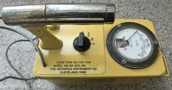
|
Geiger counters, back in those days, were put out to a common specification for the basic outward design and operational standards, but were built by the various firms that got involved inoutward design and operational standards, but were built by the various firms that got involved in the program each to its own design, electronically. This meant that any V-700 unit would look and function just the same as any other V-700 unit, regardless of the actual manufacturers, but under the skin, each maker had its own proprietary circuit design.
To make matters even more curious, certain manufacturers built multiple different models or design levels of specific devices. For example, from one manufacturer, there was a CD V-700 Model 6, Model 6A, and Model 6B. The circuits in these different design levels were not identical, with each successive sub-model having some sort of design advantage over its previous counterpart.
Of the units that were brought to me for repair, this article will discuss the Victoreen CD V-700 Model 6A Radiological Survey Meter. This unit is a two-transistor design that uses a Geiger tube as the sensing element, and originally used a corona discharge regulator tube in the high voltage power supply, which operated at about 900 volts. The unit is powered by four standard “D” cells as found in most flashlights at that time. The Geiger tube is mounted in a remote probe connected to the main unit via a thirty-six inch long cable. The probe is a nickel-plated brass tube with a window that can be opened to varying degrees to admit beta radiation. This unit will detect both beta and gamma radiation.

Figure 1 : PCB Before Repair
|
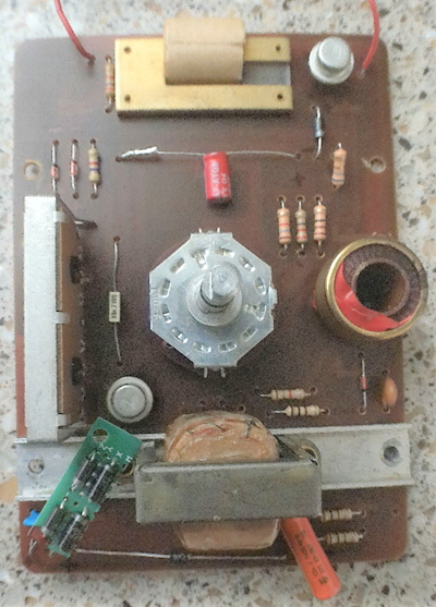
Figure 2 : PCB After Repair
|
The high voltage power supply, operating from about 850 to 920 volts, consists of an oscillator, a flyback transformer, a rectifier and a filter capacitor, as well as the 900V corona discharge regulator tube mentioned earlier. This power supply is operated from only two of the four “D” cells installed in the unit.
There is also a pulse shaping and metering circuit, supplied by the remaining two “D” cells, and using the second transistor for its oscillator. This circuit responds to output pulses from the Geiger tube, and forms amplified pulses that trigger the meter as well as the headphone circuit, where the characteristic “clicking” sound of the Geiger counter can be heard, as well as being seen on the meter.
The most apparent problem with this unit was the fact that both transistors had failed, as had the corona discharge tube. I was able to source a kit that contained all of the necessary parts including a Zener diode stack on a small PCB that replaced the corona discharge tube and now serves as the 900V regulator.
While the ceramic capacitors in this unit had not failed, I replaced them with their counterparts from the kit, as the replacements were rated for considerably higher voltages, some of which were operating at voltages very near their rated limits. The sole electrolytic capacitor exhibited severe leakage, with an ESR off the high end of the scale on my ESR meter. It too was in the repair kit, and was thus easily replaced.
The range switch was severely oxidized and required extensive cleaning and restoration. This was a job for the DeoxIT® G100L (DeoxIT Gold) cleaner and lubricant. A quarter-hour with some cotton swabs and the DeoxIT® did the trick, and the switch was restored to a fully operational condition. This might be a good point for a word or two about the DeoxIT® products that I use. I regularly use the DeoxIT® D5 cleaner and lubricant, which I purchase in an aerosol can. This is my everyday go-to product for switch and pot cleaning and restoration. I also use the DeoxIT® X10S Precision Instrument Lubricant for lubrication of such things as meter movements, tuning capacitor bearings and bushings, control shaft bushings, and so forth. However, when a really bad switch or pot shows up, I reach for the DeoxIT® G100L. This product is expensive (about $50 for a 25ml bottle), and as a result I use it only when I really need to, but when it is needed, there is no substitute! Sales talk ended…
A thorough cleaning of the contacts in the battery boxes, and a general cleaning of the exterior of the unit, and it was time for final assembly, testing, and calibration.
Testing consisted of measuring the operating voltages and comparing them to those provided on the unit schematic, which is found in the instruction manual. Next up was a check of the pulse shaping and integrating circuit using an oscilloscope. A three-volt square wave of 150 microseconds duration, followed by a -20V flyback pulse, is what we were looking for and what we found.
Calibration is accomplished simply enough, as a radioactive sample is mounted directly to the outside of the unit lower housing. The instruction manual, readily obtainable online, has calibration instructions that are well-written and easy to follow, so calibration was a breeze.
This unit turned out to be a relatively simple repair, and it was fun working on something that had a place in our national history during the Cold War era. I will write up the second unit, the CD V-715, in another article. That was a little bit different…
See you next month.
ICOM IC-3210 - July 2023
|
This month’s repair tale involves an Icom IC-3210 dual-band mobile radio (Figure 1), which came in for two separate problems. First of all, the front panel backlighting was inoperative, making it almost impossible to read the display without the use of a flashlight. The second problem was that the radio would not lock in properly on the UHF band most of
|
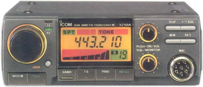
Figure 1 : IC-3210
|
the time, though occasionally it would work normally. That problem is one of a type that is normally quite difficult to locate – an intermittent problem.
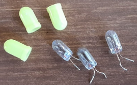
Figure 2 : Original Lamps With Boots
|

Figure 3 : Logic PCB Foil Side With Lamp Holes Indicated
|

Figure 4 : Logic PCB With Lamp Holes Indicated
The backlight problem was one that was to be expected with a radio of the age of this particular unit. The front panel on this model is backlit by a set of three T-1 12VDC incandescent lamps that are soldered in place on the front panel printed circuit board (PCB), called the logic board by Icom. Each of these lamps is covered with a yellow plastic boot (Figure 2) that provides the desired color to the illumination provided. The lamps sit down into holes in the PCB (Figure 3 & Figure 4) and have their wire leads soldered to pads on the PCB. The PCB holes index with recesses in the front panel carrier housing, directing the provided light into the rear area of the panel. All three of the lamps were burned out.
While replacements for the original lamps are readily available from standard component sources. I decided to replace them with LED’s instead, so as to preclude the probability of a repeat failure of the backlight system. In order to access the PCB and remove the failed lamps, the front panel subassembly must first be removed from the radio chassis, and then further disassembled. This involves removal of the steel frame and the plastic front cover, followed by removal of the three rotary controls. Finally, the LCD panel and its insulator can be removed by twisting the locking tabs to align them with the slots in the PCB. Once the tabs are aligned with the slots, the LCD panel can be pulled straight out from the PCB. After the LCD panel is removed, the plastic front panel carrier housing can be removed from the PCB by removing the small screws that secure the PCB to the carrier. Finally, some of the wiring harnesses can be gotten out of the way by unplugging them. As always, this is the time for some photos of the harness connections to be taken, against the future reconnection of these plugs to the main PCB.
Once the PCB is stripped down as far as is possible, removal of the lamps was a simple matter of heating their soldered lead connections and lifting the lamps out of their holes. I then cleaned the excess solder off the pads using a soldering iron and some flux-impregnated braided solder wick.
As mentioned above, I had decided to use LED’s instead of the OEM incandescent type of lamps for the replacements. I chose cool white LED’s in the 3mm (T-1) size, and I paired each LED with a 1kΩ resistor for current-limiting purposes. I removed the yellow plastic boots from the original lamps and installed them onto the LED’s. I then placed the LED’s in the lamp holes of the PCB, soldering the cathode leads to the appropriate pads. Next, I added a resistor to each of the LED anode leads, and then soldered the opposite end of the resistors to the appropriate PCB pads. Application of 12VDC from a power supply to the PCB showed that all three LED’s worked perfectly. It was time to move on to the other problem that the radio’s owner had reported.

Figure 5 : Tantalum Capacitors Removed
|

Figure 6 : Locations Of Failed Capacitors
|
I chose to tackle this problem while the front panel was still disassembled due to the fact that the most likely problem was the switch that is used to switch between bands. That switch is a 6mm x 6mm normally-open (NO) tactile pushbutton switch. When tested, the switch would make only when pressed very firmly. A normal pressing action on the switch would have no effect on the band selection. This one turned out to be a simple replacement of the switch. I desoldered the original switch, and installed the replacement, which I had on hand as it is a standard switch. Easy peasy, right? Not so much as you might think. It turned out that there was also a known problem with this radio model in that two capacitors on the main PCB are known to fail together with this switch. What happens is that two tantalum capacitors, C87 (0.22µF/35V) and C97 (4.7µF/35V) (Figure 5 & 6) have a tendency to fail with high leakage, causing the UHF phase-locked loop circuit to lose phase lock. The user causes the switch damage by repeatedly working the switch, often aggressively, in an attempt to get the radio to lock onto the UHF band. This action causes the switch to become fatigued internally, leading to the switch failure found on this unit. As a result, the switch merited replacement, as did the two tantalum capacitors. On testing of the removed capacitors, they both had extremely high DC leakage values, and had ESR readings of 14.6Ω for C97 and 9.3Ω for C87.
I next checked the memory keep-alive battery, a BR-2032 coin cell. Yes, that is correct and not a typographical error. It turns out that the BR-series of coin cells are designed for low current drain over an extended period of time. Whereas I had CR-2032 cells in stock with the right welded tabs, I did not want to change the life expectancy of the coin cell in the radio by installing a CR-2032 cell.
The radio dates back to the late 1980’s - its production was discontinued in 1990. The cell in place in the radio had the Icom part number on it, so it was either an original part or a replacement installed by an authorized service center (or someone who bought the cell from Icom). While it is possible that this was the factory cell, it is equally unlikely that it was still original after all of these intervening years. I disconnected it from the circuit for testing, and found that the open-circuit voltage was reading right about 3 volts (3.04V to be exact), which is the nominal voltage of the cell. However, when tested under load, the voltage dropped down to just over 1 volt (1.156V to be exact). Load testing of these cells is best done by installing a 100Ω resistor between the voltmeter leads when measuring the cell voltage. The resistor provides the requisite load, which really tells the story.
I keep a couple of resistors of different values, soldered between small alligator clips, on hand for just this purpose. To use them, I simply select the one with the load value that I want to use, and connect the alligator clips to the voltmeter probes. Then, whenever I measure a battery or cell with the voltmeter with the resistor clipped in place, it is automatically providing a load test for the battery or cell. You can develop a list of desired resistor values for this task by perusing the various battery or cell datasheets. The datasheet will usually provide testing information which includes the load placed on the DUT during testing.
Anyway, I ordered in the correct BR-2032 with the necessary welded tabs for this application, and when it came in, I installed it. However, I did do a load test on the new cell before installation. This one started out at 3.49V open circuit, and only dropped to 3.15V under the 100Ω load test.
After the installation of the coin cell, it was time to re-assemble the radio. Re-assembly went without a hitch, with the only point of note being that the contact fingers along the edge of the PCB where the rubberized contact pad for the LCD panel mates with the PCB need to be clean. I scrubbed them with a pencil eraser, and then removed any skin oil using 99% isopropyl alcohol (IPA) on a cotton swab. This provides for trouble-free connection to the LCD panel after handling the PCB as much as I had done. If you had inadvertently touched the business edge of the rubberized contact pad, that too should be cleaned of skin oil with some 99% IPA on a cotton swab.
Assembly is otherwise the reverse of the disassembly operation. Take care to properly tighten the control nuts on the three rotary controls, and to tighten the PCB to plastic carrier screws without overtightening and stripping them. A quick word about screwdrivers, which maybe should have been mentioned earlier. This radio was manufactured in Japan and therefore uses JIS screws throughout. As a result, JIS screwdrivers are needed to loosen any tight screws without stripping the drive recess in the screw head. Standard Phillips screwdrivers or any variation thereof will certainly cause damage to the screw heads. During disassembly, I found that one of the screws that secured the shield plate and the front panel metal frame to the radio chassis had been stripped in that manner, telling me that someone had been into this radio before and most likely had not realized at first that the screws were JIS screws. I used a specialized extractor to remove the screw, and I replaced that screw upon reassembly with a new JIS 3mm-0.5mm x 6mm flat head machine screw from my inventory.
Remember that in screw dimensioning, the first part (before the hyphen) is the nominal thread diameter, while the second part (after the hyphen) is the thread pitch reference (more about that later). The number after the “x” is the fastener length. Metric fasteners and Imperial fasteners utilize different thread pitch designation methods. With a metric threaded fastener, the pitch information is reported as the distance from the peak of one thread to the peak of the adjacent thread. Thus, a machine screw with a pitch designation of 0.5mm will have a measured distance of one-half of a millimeter from one thread peak to the next. Imperial fasteners use a system that reports the number of thread peaks in an inch of fastener length. Thus, a machine screw with a pitch designation of 32 will have 32 thread peaks in an inch of screw length. Keep in mind also that while most headed fasteners are length-measured from the underside of the head, flat-head fasteners are length-measured for overall length, including the head length.
Reconnecting of the various wire harness plugs to the main PCB is pretty much a straight-forward matter of matching the plug size to the socket size. The is only one possible mix-up, and that is with the squelch control harness plug and the speaker harness plug. This can be resolved easily if the photos recommended earlier were taken. If not, refer to the schematic diagram found in the IC-3210 service manual to determine that the squelch control harness plug goes to connector J6 on the main PCB, while the speaker harness plug goes to connector J9.
Once the reassembly is complete, it is time for a functional test of the repairs. As luck would have it, another problem became evident quite quickly. It turned out that the rotary control used as the main up/down control signal source was inoperative. As a result, frequency could not be adjusted within each band, although the radio was otherwise fully functional on each of its two bands. In a similar manner, none of the radio’s optional settings that require an up/down selection normally made via that control were operational. Thus, the tuning step intervals, the CTCSS tones, and several other functions could not be changed. The problem gets worse… it turns out that the microphone Up/Down controls were also inoperable. This would seem to point to some circuit or component that is common to both control methods. In this case, I worked through the block diagram, the unit schematic, and the X-Ray views of the printed circuit boards in an effort to try to isolate the cause of this problem. Unfortunately, all of this testing and probing led to the inescapable conclusion that the problem lies within the logic board CPU integrated circuit, a µPD75308GF-101-3B9 device that is no longer available. So… while the relatively minor faults for which the radio came in were all corrected, the radio is nonetheless still inoperable, as the VFO frequencies cannot be changed. When powered on, the radio comes up on the designated calling frequencies of 146.520 MHz for VHF and 446.000 MHz for UHF.
Continued testing showed that one of the four output strobe lines from the CPU to the control matrices was extremely low in voltage as compared to the other three strobe lines, though its signal waveform was of the correct shape - just lower in amplitude than it should have been. I also noted that when exercising any of the switches on that particular strobe line, there was no response in the CPU, as those lines were not brought to a deep low with the switch activation - they were already low, so the CPU did not see the switch activations as changes of state on those lines. Unfortunately, no ready repair was available for this problem, as the CPU integrated circuit is obsolete and is therefore currently unavailable.
Sometimes, due to the so-called “planned obsolescence” so prevalent in the output of many of today’s manufacturing plants, an otherwise great little dual-band radio is relegated to the junk pile. I will keep my eyes and ears open on the lookout for another IC-3210 that I can pick up for parts, but I imagine that to be a rather futile effort. There are surprisingly few hits on Google when searching for that model number. I cannot in good conscience charge this radio owner a penny for my time spent and for the repairs that were made, as the end result was not a working radio.
See you next month!
NanoVNA H4 Touch Screen - June 2023
|
One recent Saturday afternoon, one of our fellow Club members had cause to use the Club’s NanoVNA for some new equipment testing. Unfortunately, when he tried to operate the unit, the touch-screen feature was not working, and in fact, it seemed that the menu system was completely inoperative. I decided to bring it home with me to make the required repairs.
The Club’s NanoVNA is the H4 (Figure 1) variant which, at the time, was loaded with the DiSlord version 1.1.01 firmware dated 30 December 2021. While the firmware was most |

Figure 1 : NanoVNA H4
|
likely not the cause of the problem, as the unit had been working fine for a long while, I did notice that the firmware was about a year and a half old, which is a lifetime by today’s electronic equipment standards. I slated it for a firmware update as a part of the repair.
In testing the NanoVNA quite thoroughly, I found that occasionally, I could get the menu system to operate via the multi-function control (MFC) wheel on the unit’s top edge, after which the touch screen would occasionally operate until the next power-off. However, it was not consistent enough to say that this would be a usable work-around, so I kept on digging for an answer.
I opened up the unit and disconnected the battery and the touch screen ribbon cable. I then reseated the ribbon cable, reconnected the battery, and powered up the device. No change was evident, with the touch screen and menu system operating the same as it had before the disconnects.
A few more words about the actual behavior would seem appropriate at this point. If I was able to get the menu system to launch using the MFC wheel, it was then possible to navigate the menu using the stylus via the touch screen. It was even possible to re-launch the menu system via the touch screen, until the unit was powered off. Then the problem re-asserted itself and it was pot luck as to whether or not the menus would open via the MFC.
I turned to that giant reference resource called the internet for some help, and I came across an obscure reference in a forum somewhere - I never noticed where - that made mention of NanoVNA stability. This seemed to fit, so I looked some more into that concept - stability and how to control it. What I found was that the default settings for the DiSlord firmware versions are set to slightly over-clock the NanoVNA. I decided to slow it down a little bit and see what happens.
The clock speed of the NanoVNA is controlled by a firmware value called Threshold, which is set to 300.000100MHz by default. The Threshold setting (Figure 2) is found under Config > Expert Settings. I decided to set it down to 290MHz. Voilá! The touch screen now behaved normally in every regard! I figured that I had resolved this issue, though I still did not understand what had happened, or specifically why it spontaneously stopped working after operating for so long, but I chose not to worry about that at this point.
I next went about performing a firmware upgrade on the NanoVNA. This is a simple operation that is done using the STMicroelectronics DfuSe software. I had the software (Figure 3) installed on my PC already, so all that I needed to do was to download the newest DiSlord firmware file in the commonly-used .dfu firmware format. That filename is NanoVNA.H4.v1.2.20.dfu which indicates that the firmware is version 1.2.20, dated 12 March 2023. The various firmware files can be downloaded from https://github.com/DiSlord/NanoVNA-D/releases under the Assets listing.
To update the firmware in the NanoVNA, the device must be placed into DFU mode. Start out by launching the STMicro DfuSe software and connecting the NanoVNA to the PC via an appropriate USB cable. Then, put the NanoVNA into DFU mode by holding down the MFC wheel while powering up the unit. Note that the screen will remain black in DFU mode, but the STMicro DfuSe software should indicate that the NanoVNA is connected and accessible. The net step is to use the Choose button in the DfuSe software to open the .dfu firmware file. The software will show (Figure 4) that the firmware file was successfully loaded into the utility and that it is ready for upload to the device. Upload that file to the device by clicking the Upgrade button. Once the upgrade is completed as indicated in the software (Figure 5), power off the NanoVNA and disconnect it from the PC.
The interesting thing about this repair is that post-upgrade of the firmware, that new firmware Threshold setting was once again set to 300.000100MHz… but the unit was operating properly and with many more menu options than it had before.
OK - so slowing the clock speed solved the initial touch screen response issue in the old firmware. Of that there is no doubt. As a result, I feel comfortable suggesting that as a solution for anyone who may encounter a similar issue with the touch screen on a NanoVNA H4 and needs an immediate fix.
I also feel comfortable recommending the firmware upgrade to DiSlord version 1.2.20, as I have now installed and tested it extensively, and everything works as it should. Some of the new features include the ability to save a calibration set to the SD card, enter a custom name for any image file saved to the SD card (or simply check the Autoname check box to avoid having to enter a name - it will default to a date and time format naming convention). The new firmware allows loading an image from the SD card into the display, and there is also a Pause Sweep and Resume Sweep capability now. There are several changes to the Calibrate menu item as well as to several other menu items. This new firmware version is feature-rich and is well worth installing.
Having explored the new menu items and capabilities of the NanoVNA H4 under DiSlord firmware 1.2.20, I am happy to report that all of the new features work well, and are for the most part self-explanatory or very intuitive. This makes these new features easy to use without needing any type of documentation for them. I like the new firmware so much that I also installed it onto my personal H4 unit.
See you next month…
Brother P-Touch® 1400 Label Printer – May 2023
|
Fairly recently, I was presented with a somewhat different type of repair. One of my fellow radio Club members asked me if I would take a look at a favorite and trusted piece of his shack equipment, namely a Brother P-touch® 1400 hand-held label printer (Figure 1). The printer had stopped responding to the “Y” key, and its owner was hoping that I could repair the machine for him. Enjoying a challenge, I told him that I would take it on, but without any up-front guarantee of success.
The owner brought the machine to me, and I quickly determined that not only did the “Y” key not work at all, the other keys along the right edge of the keyboard were rather “mushy” and not crisp and quick as they should have been. I opened up the unit to find that the printed circuit board on which the key contacts were etched had delaminated at a mounting pad along its right-hand edge, directly in alignment with the “Y” key, and breaking the circuit traces for that key and one other. This was apparently a product of years of use and pressure on that portion of the board. The keyboard consists of a matrix of conductive pads etched onto the top surface of a phenolic board that also serves as a printed circuit board for some of the related circuitry. Each key |

Figure 1 : Brother P-touch 1400
|
contains a carbon button on its underside that bridges the conductive pads when the key is pressed. Simple enough, right? The problem was that the board had split between its layers (Figure 2), tearing the circuit traces on its upper surface. I was faced with a dual problem – how to first repair the delaminated phenolic board, and then how to repair the circuit traces (Figure 3) so that the machine would operate properly afterwards.
The first problem was solved with some cyanoacrylate glue, applied between the layers, with the layers then being clamped together with the broken section positioned back where it belonged. I clamped it up and set it aside to cure, having placed some waxed paper between the clamp faces and the board surfaces so that the clamp would not end up glued to the board by the excess glue squeeze-out. I then started thinking about the most effective manner in which to repair the circuit traces, assuming that the glue job would hold, of which I was not certain yet.
The most common method of repairing lifted or broken printed circuit traces, by far, is to simply scrape the trace to expose the conductive surface, and then to overlay the trace with some bare wire, and to then solder the wire to the trace. While this might work in some cases, it would clearly not be an effective repair in this situation, as one broken trace was directly in the area where the “Y” key’s carbon button would have to make contact with the board if that key were to be pressed. Any raised area of the board would be problematic in allowing the carbon button to successfully bridge the pads, which actually contain interlaced “fingers” (Figure 4) rather than being geometrically shaped areas. I needed a better solution.
The next day, still unsure of how to repair the traces, I removed the clamp and waxed paper to find that the board was indeed back into a semblance of its original condition. I used some acetone on a cotton swab to clean the squeezed-out CA glue from the board surface in the area of concern, and the board was ready for trace repairs to begin. Still not having a repair scheme in mind, I put it aside for the day and moved on to something else, having already sent photos of the damage to the machine’s owner and having told him that a repair might not be feasible. I went to bed that night thinking about the problem.
At some point during the night, and driven by some unknown and not understood “force”, I hit upon an idea that might just work. I had read a while back about pens that write with conductive ink, which contains powdered silver in a volatile carrier. It was well worth a try, so I ordered one of the pens from Amazon and waited another day for it to arrive. Lo and behold, when I tried the pen on some paper, and then measured the resistance of the drawn lines, I found them to be very low impedance traces, and with almost no appreciable height on the paper surface.
I tried some basic experiments to determine the current-carrying capability of the ink, and found that I could easily pass 500mA through a trace that was two pen-points in width. This looked very promising indeed! I decided to try the ink on the phenolic board.
To make this idea work, I would have to expose some of the conductive surface of the existing traces for the ink to connect into the original circuit properly. That was a chore best done with the edge of a hobby knife blade, and that is exactly how I achieved the exposure that I needed. I then laid the ink down in place (Figure 5) over the almost invisible cracks in the repaired surface of the board, and checked the results with an ohmmeter. So far, do good. Now for the acid test. Will the key work when coming into contact with the ink and the original traces? A quick test with the keyboard membrane laid over the board proved that it would actually work as intended.
After that, all that was required was to reassemble the machine with the repaired PCB (Figure 6) and to do a final working test of the entire keyboard. That post-assembly test proved successful, and so the repair was complete. The lessons found in this repair are two-fold.
First, think out of the box when faced with an unusual problem, as unusual problems often require unusual repair methods.
Second, do not give up too easily. Plan for the worst, but work towards the best, and let your unconscious mind work on the problem for a while.
You might just know how to achieve a repair, even if you don’t know that you know how to do it!
See you next month.
Icom ID-800H – April 2023
|
Sometimes, finding the cause of a problem can be more than the repair technician is up to. At those times, the technician has to be careful not to do any harm to the equipment and cause further failures while trying to ferret out the root cause of the initial failure. Sometimes, like the infamous Zorro, the technician leaves his/her mark in the night, gives up, and moves on. That is when the failure becomes another technician’s problem to solve.
|

|
A little while ago, I got an email from a ham out in Cleveland, Tennessee who asked if I would be willing and able to take on a “mystery” repair on an Icom ID-800H 2-meter/70-centimeter dual-band mobile radio (Figure 1). The unit had an intermittent fault that two other shops had attempted to repair and both gave up without finding the problem. In addition, one of the two shops caused an additional failure, which we will get into in a little while.
The original problem was related to the occasional and unpredictable blown fuse on the incoming power line. The ID-800H was vehicle-mounted in a 2022 Peterbilt 579 (Figure 2) Class 8 truck-tractor. The secondary problem was a lack of audio from the radio unless an external speaker was installed and connected. This problem showed up when the radio came back from the second repair shop. The owner is an over-the-road long-distance trucker who has historically had his radio - CB’s and ham - all repaired at truck stop radio shops.
When the problem first appeared, the owner took the radio to a radio shop at a truck stop in Carlisle, PA. Of course, as nothing was actually repaired other than replacement of the blown fuse, the problem eventually re-occurred. At this point, the owner replaced the fuse himself, and the radio worked as it was intended to, for a while. At some point, the owner happened to have some time to kill while in Kenly, NC, so he took the radio to a radio shop at a truck stop there. This time when he reinstalled it in the truck, it worked again, except that there was no audio from the internal speaker. This was annoying, and the owner assumed that the repairman simply forgot to reconnect the speaker wire harness to the mainboard on re-assembly. However, due to the ambient noise level in the truck, he customarily used an amplified external speaker anyway, so he didn’t fret too much about it. Needless to say, the radio was still blowing fuses at random times.
Fast-forward to the first of the year. As of 1 January 2023, the owner came off the road and began operating as a local, home-every-night driver, and the radio came out of the truck to be used in his shack at home, except that it still had that pesky fuse-blowing problem, which is where I entered the story.
The owner explained the entire history to me, and after some judicious questions, I determined that the fuse most often blew while the truck was in motion, though it would occasionally blow when the vehicle was stationary. He wanted me to find and fix the fuse blowing issue once and for all… and oh yeah - plug in the speaker, too. He shipped the radio to me, but he did not include the power cable, so I had to use a bench cable with a fuse holder (Figure 3) to power the radio for testing, to which I added Anderson PowerPole® for my own convenience.
I put the radio on the bench and connected up the incoming power, a dummy load, and an external speaker… and the radio worked normally. I then decided to connect it to an antenna - my trusty Ed Fong J-Pole - and to use it on the Tuesday net. The radio worked flawlessly, albeit through the external speaker. I decided that I would try to emulate the rough ride of the truck where the radio used to live… I picked it up and I shook it while it was operating. I shook it, I banged on it, I bounced it on a stack of towels… and nothing. It never missed a beat. Next, I tried some “unusual attitudes” as we used to call it in flight school. I started twisting and turning the radio while bouncing it on the stack of towels. Finally, when I stood the unit up on end with the front face upwards, and bounced it hard on the towel stack, it finally blew the fuse. I replaced the fuse and tried the same thing again, and once more the fuse blew with the same maneuvers.
So, what did I prove? Well… I showed two things to be true :
- That the fuse did blow after some violent jarring of the radio.
- The behavior was repeatable.
Now it was time to open up the radio and the service manual, and to start investigating the internals. It just so happens that I have one of these radios myself, which may come into play for some comparisons, if necessary.
I disconnected the radio and opened it up, and the very first thing that I noted was that the speaker wire harness was indeed connected to the mainboard. This meant that I would need to dig a bit into the audio issue as well, to get to the cause of that problem. More on that later.
As usual, I began by looking for any visible indications of something burnt, arced, or otherwise indicating a short circuit, but nothing jumped out at me. I removed the RF shield from the mainboard to look underneath it as well. Finding nothing the easy way, I decided to emulate my vigorous treatment of the radio. With a new fuse in the power wire fuse holder and the unit power on, I began to gently poke and prod various points in the radio using a plastic alignment tool as the prod. Nothing happened until I prodded the wire harness for the cooling fan. As soon as I touched this wire pair, it arced against the chassis rear heat sink and the fuse blew. Success!
Closer examination revealed a chafed area (Figure 4) in the red wire to the fan, exposing the bare wire inside the red insulation. I surmise that this wire would, with enough of a jar to the radio, move just enough to short against the heat sink, causing the fuse to blow. A look at the schematic shows that the fan is fed almost full supply voltage, dropped only by a 6.8Ω resistor in series with the fan positive lead. The fan supply, on lead HVI, traces back from the 6.8Ω fuse R102 directly to the incoming 13.8VDC power inlet. Fan control is all done on the fan’s negative lead. Thus, shorting the fan’s positive lead to ground is tantamount to placing a direct short on the positive power feed to the radio, causing the fuse to open.
The repair was fairly simple. Using the tip of a hobby knife, I gently lifted the latch of the red wire terminal in the fan harness plug, and pulled the wire and terminal from the plug (Figure 5). I then slipped a short piece of narrow heat shrink tube on the wire and hit it with hot air from the heat gun. Once the HST was shrunk in place, I inserted the terminal back into the plug (Figure 6). After that, it was a simple matter to re-mount the fan and plug it in onto the mainboard.
Now it was time to look for the audio problem. As a refresher, the radio had audio only via an external speaker. No sound came from the internal speaker, which was plugged in onto the mainboard in the correct location. The owner had thought that perhaps the last repairman had forgotten to connect the speaker harness, but that was not the case, as I discovered. I had to start somewhere, so I started at the speaker connector on the mainboard. To my surprise, there was a strong audio signal there at the speaker header. Thus, the problem had to be in either the speaker or its connecting harness. I took a “AA” battery that I keep on hand with a clip lead soldered to each end, and I did a momentary “scratch” test of the speaker, which responded with a typical characteristic static scratch. The speaker coil was intact, which narrowed down the problem. It had to be a harness issue.
I took a good close look at the plug end of the harness and found that one of the wires was out of the plug body, and therefore was not able to make contact with the header pin. My guess is that when the last repairman disconnected the speaker on opening the radio, he pulled the wire from the plug (Figure 7) and did not notice it. I certainly did not notice it until I had reason to take a good look at the plug. I pushed the wire all the way into the plug body and connected the harness. Magic! The dead audio was once again alive.
I reassembled the radio and once more subjected it to a violent thrashing in an attempt to blow another fuse, but failed to do so. I took that as a sign that the repair was effective, so I boxed it up, less the power cord, and shipped it back to Tennessee, together with my invoice and two spare fuses.
What lessons can be learned from this repair? I see a couple of them. Let’s take them one at a time, and explore their validity and value.
First off, I think that the fix isn’t made until the repair person actually finds the cause of the problem. Fixing a symptom, in this case the blown fuses, does not repair the equipment, not so long as the root cause has not been located. Without correcting the root cause, the symptom is bound to re-appear at some point in time. The fact that this radio was riding around in an eighteen-wheeler, and taking an aggressive hammering as the truck traveled America’s highways and byways, meant that the unit was being put through some unusual operating conditions. It was when I emulated that pounding ride that I was able to reproduce the symptom, reliably and repeatedly. Think outside the box and consider all operating conditions when tracking down a symptom like this one.
Second, it is obvious to me that the second repair shop failed to do any kind of active post-repair testing of the radio, because if such testing had been done, it would have been obvious that a new problem had been introduced in that the speaker audio output was nil. Perhaps the repairman thought that the radio had been like that when it came to him, but the owner says otherwise. It is important that the repaired radio be put through all of its paces post-repair just to make sure that something like this has not happened. It is understandable how it happened; it is inexcusable that it left the shop like that.
I am not saying that my repairs are perfect - I am human, and so I will make mistakes and miss things, as I have in the past. However, any shop should be able to pick the low-hanging fruit and fix the easy ones. The more difficult ones just take a little bit longer, or maybe a lot longer.
See you next month!
Icom ID-4100A – March 2023
|
Sometimes, you have to repair - or at least I have to repair - my own equipment. And, sometimes the old adage about “getting what you pay for” is true. In this case, it certainly came true. I had been having occasional problems with my Icom ID-4100A (Figure 1) powering itself off, most often at the end of a transmission, but occasionally during receive operations. |

Figure 1 : Icom ID-4100A
|
There was no rhyme or reason to when this would happen. It might happen twice during a net, or it might go several weeks without occurring. I was always able to restore the radio to operation by power-cycling the power supply, and I was therefore half convinced that the problem was internal to the radio, so I set about trying to locate the problem.
My first step was to take the ID-4100A out of service. I unplugged the power cord at the “T” connector (Figure 2) that is so common on mobile radios today. The radio that I was swapping in there temporarily, an Icom ID-800H, had the same type of power cord, so it was a plug-in replacement as far as the connections went - power cord and antenna cable.
I fired up the ID-800H and all was well. I set the ID-4100A aside for repairs when I could fit the job into my schedule, reasoning that there was no hurry as I had yet another 2-meter set available if the ID-800H should fail, a Yaesu FT-1900. In this way, I should not have to resort to my handheld for the nets, right?
Two weeks go by, meaning four nets in which I participated, for two of which I was the Net Control Station, and all was working well. I sat there thinking through the ID-4100A problem, and poring over the schematic and block diagram, looking for the most likely place to start in troubleshooting the shutdown issue, but had not yet reached any definite conclusions.
Another week goes by, with two more nets. During the Thursday net, the old faithful ID-800H shut down, exactly as the ID-4100A had been doing! Stop the truck and back it up. I concluded now that the problem was not in the radio after all. At this point, I began suspecting the power supply instead, as it was common to the two radios. I decided to watch carefully the next time the radio went dead to see how the power supply behaved. I got a bit of a surprise doing that.
The next time the radio fell dead was the Tuesday net two weeks later. Throughout the net, I sat there staring at the front of the power supply, studying its backlighting and the output monitor meter. What I saw there puzzled me for a few minutes… the power supply showed a momentary spike in output current just as the radio died, but then dropped to a zero-current state.
The output voltage had momentarily sagged a little bit, but then jumped right back up to the normal 13.8VDC available output. This told me that the problem was neither the radio nor the power supply, but something in between them. The only thing between the power supply and the radio was the six-port Powerpole® distribution block that I had mounted behind the desk, and of course the power cables themselves. No fuses had blown through all of this, with either radio.
I went to the Powerpole® distribution block and carefully examined both it and the power cords connected to it. Much to my surprise, I found that the port to which my 2-meter radio was connected looked melted, very slightly on the black connector shell, but quite heavily on the red shell (Figure 3). This melting had occurred on both the cable end (Figure 4) and the distribution block port. I disconnected the cable from that port and got another surprise. Inside the red shell of the cable, the contact was not all the way out to the end of the connector shell as it should have been. Instead, it was pushed back a little bit, enough to cause the connection made when the plug bodies were joined to be somewhat less than optimal. Apparently, this connection would occasionally open, usually when heavier current was drawn during transmission. The heat caused by the resistance formed there is what melted the connector bodies.
This particular cable was an ebay.com buy that I picked up before I got my Powerpole® assembly kit in house. I needed a power pigtail for the mobile-type radios, so I bought a couple of inexpensive ones on the auction site.
My guess is that the actual contact was never fully inserted into the connector body far enough to lock into place. It simply pushed away from its mating contact, maintaining a light touch with its mate, but opening up under load. This caused me to inspect the second cable that I bought at that time, but it was assembled correctly, with the contacts in place where they belonged.
The fix for the cable was simple. Cut off the melted connector and crimp on a new pair of Powerpole® connectors. I keep the Powerpole® parts on hand, so that was no problem. The repair to the distribution block was not quite as simple.
The distribution block has a metal cover secured in place by four small flat-head machine screws, so disassembly was easy. I removed the screws and lifted off the cover, exposing the inside of the unit. Inside, there was a small printed circuit board (Figure 5) having bus bars along its outer edges to help handle the rated current of the unit. Each of the Powerpole® shells was installed to a blade-type contact that is soldered into the PCB. I fooled around with trying to release the contact from the body and to slide the body off, but that was going nowhere fast. Ultimately, I decided to try a more direct approach. I took a pair of pliers and simply crushed the melted red connector body, causing it to separate from its contact a bit.
Then it was just a matter of using pliers to grip and wiggle it off the contact, sort of like pulling a tooth (Figure 6). After that, all that was left was the job of forcing a new connector body down in place of the melted one. The black connector body was intact, so I was able to leave that one alone.
After the connector shell was replaced, reassembly of the distribution block was the reverse of the disassembly procedure. The only tricky part was reinstalling the three miniature truss-head machine screws that secure the PCB to the lower enclosure half, as they are buried down between the Powerpole® shells.
With the distribution block repaired and reassembled (Figure 7), it was time to put it back into service, which I did. The new connectors on the power cable, properly assembled this time, worked as they should, and the problem of the dead radio has not occurred since the repairs.
The lesson in all of this is to inspect every piece of kit that you buy, because even “brand new” items might be defective. Had I inspected this cable before use, I may have noticed that the contact was not seated and I could have corrected it. All that would have been needed was to properly seat the contact in the connector shell by pushing in until it clicked into place. I failed to do so, and ended up with a mystery to solve as a result.
See you next month!
MFJ-259 HF/VHF SWR Analyzer - February 2023
|
This month’s case history is a slight departure from the norm, in that it involves the repair of a piece of test equipment. Notably, the unit under repair is one that I had already done some repair work to, prior to donating this piece to the Club for the test and repair bench. On a recent Saturday afternoon, Frank N3PUU had occasion to use the MFJ-259 SWR Analyzer while setting up the VHF station for an upcoming contest. Unfortunately, the unit did not operate as expected, and Frank left me a note to that effect. Naturally, I picked up the unit and brought it home for repair. What should have been a quite simple repair job turned into a little bit more than I had bargained for. The reported problem was that the meter was not reading, meaning that there was no indication of the tested SWR value. A quick check verified the condition, showing that the LCD panel was operational as to displaying the test frequency, but the meter movement was inoperative. However, I noticed that the meter came alive when I happened to jar the unit when I went to place it on the bench. That gave me a hint as to where to look for the problem. |

|
Diving in “under the hood”, so to speak, I quickly found some cracked solder joints on the unit’s main printed circuit board. There are two meters on the front panel of this unit. One is the SWR meter, and the other is a resistance meter. These two meters are connected to the main PCB via a three-wire harness with a 90° plug at its end (Figure 1). The plug connects to a three-pin right-angle pin header on the PCB. It was this header that had the cracked solder joints (Figure 2). A simple fix - I simply reflowed the solder on those pins and the meters worked as intended. However, I did not stop there.
You see, I had been bothered by this unit ever since I put it on the test and repair bench. I felt that I did not do as thorough a refurb job on this unit as I could have, and this was borne out by the fact that Frank had trouble with the unit when he tried to use it. One of the items that I had intended to replace but did not was the SO-239 jack on the top of the unit. I decided to go ahead and give the whole unit a closer look and to replace the SO-239 jack.
Replacement of the SO-239 connector requires removal of the main PCB, which in turn requires desoldering of the two pushbutton switches and the BNC jack on the unit’s upper surface. The SO-239 itself is connected to the main PCB in an unusual fashion. The center pin of the SO-239, when the main PCB is in place, sits about an eighth of an inch above the PCB. That gap is simply filled with solder at the factory. Each of the two mounting screws used for the SO-239 has a solder lug installed under its nut. The lugs are then bent over to reach the main PCB and are soldered to pads on the PCB. These solder lugs also do not quite reach the board surface, and so their gaps are also solder-filled in production (Figure 3). Large solder bridges of this type are prone to cracking with time, a condition with which I was not happy. I therefore decided to correct this as well.
Another poor manufacturing technique, in my view, was the manner in which the BNC jack and the pushbutton switches were connected. The two pushbutton switches are normally-open switches that, when pressed, connect their respective circuits to ground. The way that MFJ chose to implement this was to bend one solder lug of each switch over and solder them to the solder lug under the nut on the BNC jack (also shown in Figure 3). It was a stretch at best, and it put undue stress on the bodies of the pushbutton switches. As it turned out, when I removed these switches, I found that the bodies of both switches were cracked. Solution? Two new switches… which turned out to be an adventure in and of itself.
I installed the new SO-239 to the enclosure. Then, I went over the main and display PCB’s carefully, touching up any solder joints that looked the least bit suspicious. I then installed the main PCB to the enclosure, and I added lengths of bus wire between the mainboard solder pads and the SO-239 center pin and also at the solder lugs on its mounting screws (Figure 4). Next, I installed the BNC jack and the two pushbutton switches, wiring them up to the main PCB as they were originally. I added some bus wire to connect the grounded sides of the pushbutton switches to the BNC jack ground lug to make it a more comfortable fit. Now for the moment of truth.
I connected the battery banks (there are two of them) and powered up the unit, only to find that the LCD panel was not working. Now what? Did I damage the LCD panel in doing my solder touch-ups? I did not think so, but I went ahead and removed the main PCB again so that I could inspect the display PCB carefully. As luck would have it, I found nothing wrong there.
I sat back and thought about it a little bit, and then I decided to eliminate possibilities by testing the unit operation at each step of assembly. I installed the main PCB and checked the LCD operation, finding that it worked normally. I connected the SO-239 jack and again checked the LCD operation, and it worked just fine, which makes sense, as the jack was open.
So, next I wired up the BNC jack, and as expected (as this jack too was open), the LCD operated as it was meant to. I then connected the first of the two pushbutton switches, the one labeled “GATE”. Once again, the LCD panel worked normally. Finally, a bit confused, I connected the “INPUT” pushbutton switch. Of course, now the LCD panel did not work.
As mentioned earlier, the pushbutton switches are normally-open switches, so connecting that last switch should not have made any difference, but it did… which meant that the switch was obviously not open! I checked the switch with an ohmmeter, and sure enough, it was a normally-closed switch that had somehow gotten mixed in with my supply of normally-open switches. Swapping out that switch for another (verified NO) switch from my stock solved the problem (Figures 5 & 6).
The lesson to be learned from this repair is actually a dual lesson.
When things don’t work out the way that you expect them to, think it through and carefully go back over what you have done and especially any changes that you have made.
A thorough search will usually turn up the culprit.
See you next month!
I installed the new SO-239 to the enclosure. Then, I went over the main and display PCB’s carefully, touching up any solder joints that looked the least bit suspicious. I then installed the main PCB to the enclosure, and I added lengths of bus wire between the mainboard solder pads and the SO-239 center pin and also at the solder lugs on its mounting screws (Figure 4). Next, I installed the BNC jack and the two pushbutton switches, wiring them up to the main PCB as they were originally. I added some bus wire to connect the grounded sides of the pushbutton switches to the BNC jack ground lug to make it a more comfortable fit. Now for the moment of truth.
I connected the battery banks (there are two of them) and powered up the unit, only to find that the LCD panel was not working. Now what? Did I damage the LCD panel in doing my solder touch-ups? I did not think so, but I went ahead and removed the main PCB again so that I could inspect the display PCB carefully. As luck would have it, I found nothing wrong there.
I sat back and thought about it a little bit, and then I decided to eliminate possibilities by testing the unit operation at each step of assembly. I installed the main PCB and checked the LCD operation, finding that it worked normally. I connected the SO-239 jack and again checked the LCD operation, and it worked just fine, which makes sense, as the jack was open.
So, next I wired up the BNC jack, and as expected (as this jack too was open), the LCD operated as it was meant to. I then connected the first of the two pushbutton switches, the one labeled “GATE”. Once again, the LCD panel worked normally. Finally, a bit confused, I connected the “INPUT” pushbutton switch. Of course, now the LCD panel did not work.
As mentioned earlier, the pushbutton switches are normally-open switches, so connecting that last switch should not have made any difference, but it did… which meant that the switch was obviously not open! I checked the switch with an ohmmeter, and sure enough, it was a normally-closed switch that had somehow gotten mixed in with my supply of normally-open switches. Swapping out that switch for another (verified NO) switch from my stock solved the problem (Figures 5 & 6).
The lesson to be learned from this repair is actually a dual lesson.
- First, I should have done a more complete job on this unit the first time around, before I put it on the Club’s test and repair bench.
- Second, and more to the point, remember that each and every “repair” that is made can actually introduce a previously non-existing problem.
When things don’t work out the way that you expect them to, think it through and carefully go back over what you have done and especially any changes that you have made.
A thorough search will usually turn up the culprit.
See you next month!
Henry 1KD-5 Amplifier
Henry 1KD-5 Amplifier - January 2023
Let me start out this month’s case history with an apology. No repair should take as long as this one (and one other, to be discussed in another article) did. There is no real excuse other than that the job was a bear to do, and I kind of dragged my feet on digging into the guts of this thing. I am talking about the Henry Radio 1KD-5 HF linear amplifier. This was a circa 1977 model, heavier than you can believe, with a one-tube grounded-grid circuit. The tube is a PL3-500ZG tube of about four and a half inches diameter, nestled inside an external glass bell chimney. The tube socket is buried deep inside the unit, behind a board that carries the tuning coils for the amplifier.
I am getting ahead of myself. Let’s start at the beginning. The owner brought this unit to me, explaining that the tube would light, and then go out, then light again, and then go out, and would repeat this behavior while switched on. He also told me that he was in no hurry to get it back.
I set up my 30A 230V outlet with the correct receptacle to match the Henry’s power cord, and fired it up to confirm the reported behavior. It took just about a minute or so before the on/off action became evident, so I set out to find the cause. As it turned out, that was the easy part. Some gentle pressure on tube while it was out would cause it to light up again.
The problem was that the tube socket, a humongous ceramic thing about three inches square and about three-eighths of an inch thick, had fatigued with age and the effects of heat. The result was that the contacts that grip the tube pins had relaxed quite a bit - enough so that when they got hot, the circuit would open until they cooled down, at which time the circuit would close and the process would repeat. Solution? A new tube socket.
I tracked down a source for the socket, but I had to wait for the socket to come in from China, and I had to order two of them at an exorbitant price to get the one that I needed. I buttoned up the amp and set it aside to wait for the part to come in.
Fast-forward a few months. I have the part in hand, and I finally put the Henry back on the bench. Major disassembly of the unit was required to enable access to the tube socket. I removed the glass chimney and the tube and set them aside for safe-keeping. The chimney is probably irreplaceable at this point, and the tube runs anywhere from two to four hundred dollars, depending on availability and seller. I did not want anything to happen to them!
After removal of the sheet metal covers and shields, I had to laboriously remove the forced-air cooling system fan and motor. Next, it was necessary to dismount the tuning coil board and carefully move it out of the way. A large toroidal transformer was next to be removed for access to the tube socket, which had two of its heavy wire leads soldered to the tube socket terminals. My 240-watt soldering gun was required to desolder these connections. Now I was able to get to the tube socket and ground lug mounting hardware and remove the machine screws, lock washers, and nuts. Finally, again using my 240-watt gun, I was able to desolder the capacitors from the connecting tabs of the tube socket and lift the socket out.
At the solder station, I moved the ground lugs from the old tube socket to the new one. I also drilled the tube socket solder lugs as necessary for the heavy wire from the toroidal transformer to fit. Then it was time to reassemble the whole shooting match, which was quite a tedious task due to hardware locations and difficulty in reaching some of the screws to install lock washers and nuts on them. I finally got the tube socket mounted, and then soldered its capacitor connections in place. I reinstalled the toroidal transformer and soldered its leads to the tube socket.
Reassembly of the rest was the reverse of the disassembly procedure, with the exception that I replaced many of the sheet metal screws due to their holes having been stripped or worn oversized.
After final reassembly, it was time to test and align the amplifier, which went exactly according the manual instructions with no surprises. All in all, it was a rewarding repair, though I could never charge the owner the full amount of time spent on the unit.
Sometimes, repairs are just tedious replacement of connecting parts rather than active or even passive components. This was one of those times. None the less, it was a necessary repair in order to bring the amplifier back to operational status.
See you next month!
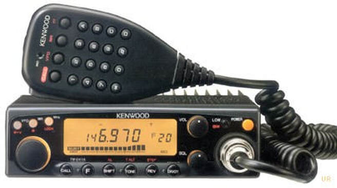
Kenwood TM-241A
Kenwood TM-241A 2M Transceiver - December 2022
Every now and then, a repair comes along that is both easy and difficult at the same time. This month’s repair case history is one of those occasions. This is the story of a simple - and not so simple - repair of a Kenwood TM-241A fifty-watt 2-meter mobile transceiver.
The radio came to me with the complaint of being inoperative on transmit, which was easily verified with a simple output test into my Bird 43 directional wattmeter and a dummy load. The Bird 43 showed zero output power from the radio. During this test, however, I also noted that the unit failed to maintain its last-used settings, which told me that there was a second problem with the radio, and therefore the need for some deeper troubleshooting.
Armed with a TM-241A service manual and schematic, I set out to isolate the output power problem first. It took only a few minutes with an oscilloscope to determine that the signal was present at the input of the final amplifier, but that there was no output from that amplifier stage. A quick check of the power supply voltages to the final amp IC (Kenwood calls this the power module) showed that the operating voltages were correct, meaning that the IC was most likely a failed device. A quick online search showed that the power module, a Toshiba S-AV17, was available from many sources, including East Coast Transistor, an authorized Kenwood parts distributor. In the interest of sticking with original factory replacement parts, I ordered the IC from ECT and waited for it to come in.
Before ordering the IC, I went ahead and checked out the most likely cause of the radio failing to store any settings - a failed memory “keep-alive” battery. Kenwood did not make it very easy to replace this battery, which is a CR2032 coin cell with an insulating outer ring and welded tabs for connection to the printed circuit board. When installed, this coin cell is sandwiched between two insulators, one of which is double-sided adhesive foam which is used to affix the coin cell to the PCB.
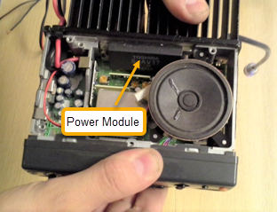
|
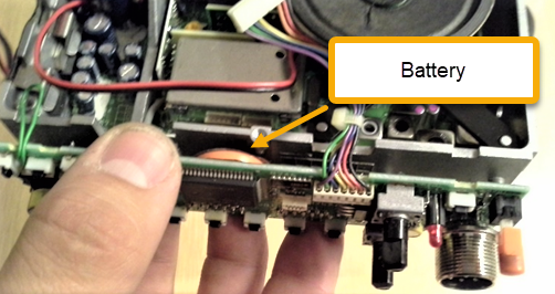
|
Accessing the battery is the not-so-easy part and involves removal of the front bezel of the radio, followed by the removal of a metal structural cover, and finally the front panel display unit printed circuit board. At this point, the battery voltage can be measured easily. When measured in-circuit, the coin cell showed a voltage of only 0.36 volts. With the battery basically “dead”, it was necessary to continue the disassembly. To do so, the main front panel PCB is removed from the chassis to allow access to the coin cell, which is mounted between this PCB and the main chassis. Care must be taken when de-soldering the coin cell so as not to overheat and damage the PCB.
An important point is to be certain to use JIS screwdrivers for this job, especially for the tiny screws that secure the metal front structure to the main chassis. It is extremely easy to strip the heads of these screws if the wrong screwdriver is used. Polarity alignment of the coin cell is aided by indications on the PCB referring to the + and - terminal connect points.
I ordered the coin cell from East Coast Transistor in the same order as the power module, and then I sat back and waited for the parts to come in. Delivery took eight business days. The parts arrived well-packaged and in good condition, though they had to travel via ground transportation due to the fact that the coin cell is a lithium battery and thus falls under certain transportation restrictions.
Installation of the coin cell and reassembly of the front panel was basically a reversal of the disassembly process. I noted that the control pushbutton extenders have a tendency to fall out when reassembling the unit. Apart from that hiccup, it is a straightforward process.
Installation of the power module, on the other hand, required removal of the main PCB from the radio chassis. I had elected not to remove this board until the new parts arrived, primarily so that the removal procedure would be fresh in my mind when it came to reassembly time.
I had taken several photographs prior to disassembly, which is a standard practice for me. This provides a reference for reassembly. In this case, it helped me to resolve a puzzle in that there is one plug with seven wires for which I could not seem to find the connect point. For several minutes, I struggled with trying to remember disconnecting the plug, but I simply did not remember unplugging it. Finally, by referring back to my photos, I realized that this is a plug that goes nowhere. It was simply hanging free underneath the loudspeaker behind the front panel. The other end of this harness is a seven-wire plug that connects to the front panel PCB.
Removing the PCB is not complex at all, and replacement of the power module on the PCB requires the normal care about excessive heat. Be aware that there are two mounting tabs on the S-AV17, which are secured to the rear of the chassis via machine screws, thus providing heat sinking for the IC. When reinstalling the PCB with the new power module, be sure to coat the rear surface of the IC with silicone thermal transfer grease for best heat transfer to the chassis. Again, be sure to use a JIS screwdriver for this task as well.
After reassembly was completed, it was time to test the operation of the repaired unit. The first thing that I checked was the ability of the radio to “remember” the last used settings. This was no problem; all worked as expected. Next up was the power output test. When tested with my faithful Bird 43 into a dummy load, the radio showed an output of >47 watts into a dummy load.
While the customer had made no mention of the settings memory issue, I would not have considered the radio to have been repaired completely if the battery had not been replaced. Had the customer squawked about the additional and not requested repair expense, I would probably have attempted to work out a parts/labor split with the customer for that specific part of the repair bill. As it turned out, the customer was satisfied with the overall repair and its cost as presented.
The moral of the story here is that there is often more to repair than just what the customer reports. A thorough repair tech will go the extra mile, though it is usually best to discuss any additional repairs with the radio’s owner before proceeding with those additional repair items.
See you next month…

ICOM IC-706 HF/6M/2M Transceiver - November 2022
Sometimes you wish that the customer would just be honest with you and tell you what really happened, and this month’s At the Repair Bench is an example of one of those times. It all began with a phone call from a gentleman out in western Pennsylvania. I should have realized that something was wonky when he couldn’t tell me who it was that referred him to me - or maybe he wouldn’t say. Anyway, he asked if he could ship his faithful Icom® IC-706 to me for repair, saying only that the front panel was “dead”. Naturally, I agreed to look at it, so he shipped it in.
He did an over-the-top job of packing the radio and mic, going so far as to buy some Lowe’s sheet foam and cut custom blocks to surround the radio, and then gluing the blocks together to make two half shells that fit the radio quite well, and also fit the carton perfectly. Kudos on that part! He lost some points, however, when I got into the repair… but I am getting ahead of myself.
After unpacking the radio, I put it on the bench and connected it to my power supply and dummy load, and powered it on… or at least I tried to power it on. Nothing happened. The unit was stone cold dead and unresponsive. I took the cover screws out and lifted the top cover, and I saw immediately what the problem was.
The Icom® IC-706 has a removable front panel, which connects behind the panel to a set of eight spring contacts, which in turn connect to the main PCB via a “flex circuit” or Kapton cable. Connection to the main PCB is made through the use of a top-entry edge connector that is surface-mount soldered to the main PCB. This connector was off the PCB and floating free inside the radio, tethered to the end of the Kapton cable.
Here is the part where the owner lost points… someone had been inside the radio and most likely pulled that connector off the board. How do I know this? Simple… the speaker connection (the speaker is mounted to the top cover) was unplugged.
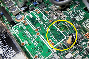

The repair was simple enough. Fortunately, no damage was done to the PCB - all of the pads were intact and in fact had plenty of solder on them. All I had to do was to reflow the solder on the connector pins once I put the connector in position. Of course, I had to remove the FL-100 CW Narrow Filter and the FL-223 SSB Narrow Filter to allow clear work access to the connector location on the PCB. The Kapton cable itself was unhurt, so after I resoldered the connector in place, I was able to simply re-insert the Kapton cable into the connector slot.
Was it embarrassment? Was it ignorance? Who knows? All that I know is that the radio performed properly once the repair was made, and I repeated the inbound packing job for the outbound trip back to the owner. A simple repair with a nebulous cause… but one thing is certain. That connector most likely did not fall off by itself.
I would much rather have the customer tell me the truth as to what is going on when a unit comes in for repair, as it takes a lot of the guesswork out of the equation. See you next month!
Heathkit® HP-23B Power Supply - October 2022
Every now and then, I will come across a repair that should have been avoidable with proper equipment maintenance. Unfortunately, some maintenance is beyond the skill set of the equipment owner. This month’s repair is just such a repair.
The Heathkit® HP-23B is a multi-output power supply used in conjunction with several of that company’s ham radio equipment offerings. The PSU provides outputs of 700VDC at 250mA, 350VDC at 150mA, 250VDC at 100mA, -100VDC at 20mA, and 12.6VAC at 5.5A. The incoming power is a standard 120VAC at about 350 watts. The unit is heavy, weighing in at about sixteen pounds.
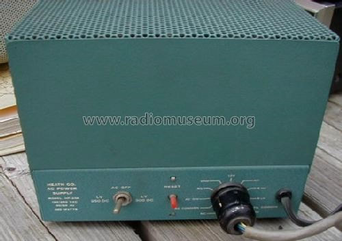
www.radiomuseum.org
|

www.radiomuseum.org
|
This particular HP-23B came to me with the complaint that it would repeatedly trip the chassis-mounted 2.92-ampere circuit breaker. The owner would press the reset button, and almost immediately it would trip out again. This behavior led me to believe that there was either a dead short circuit somewhere, or a condition that would mimic a short circuit very closely. Time for some detective work.
The circuit breaker is installed in the power transformer primary winding circuit, so I started out by applying some judicious use of the ohmmeter to the primary circuit, only to find that all was as it should be. No problem there, so it was off to the secondary side.
I decided to eliminate the simplest circuit first, which is the 12.6VAC output. This circuit is simply taken from an isolated secondary winding and carried to the output plug as the two secondary leads from the winding - no additional components. There was no short circuit there, and the winding resistance was reasonable. I moved on to the DC outputs.
The three DC output circuits are easily isolated by opening a single wire lead in each circuit, which would then allow for resistance readings to ground at various points in those circuits. It did not take very long to identify an “almost” shorted 125µF filter capacitor in the medium/low voltage output circuit. This capacitor had extremely high leakage and would obviously require replacement.
I next removed and bench-tested all of the electrolytic capacitors in the unit, and I found relatively high leakage in three of the four 125µF filter capacitors and in one of the 40µF electrolytics used in the -100VDC bias circuit.
|
There is a company called Hayseed Hamfest (www.hayseedhamfest.com) who provides re-cap kits for this power supply. The beauty of their kit is that the unit retains its original appearance, though it functions like brand new. The kit is offered in multiple formats - either with or without the smaller capacitors, and in standard or in increased working voltage versions. I ordered up the standard voltage kit in the complete (all capacitors) version and sat back and waited for it to come in. |
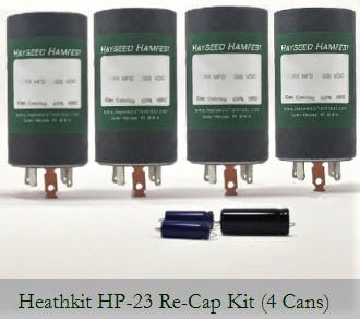
|
The installation of the capacitors was a straightforward repair, as all of the parts are intended to fit exactly in place of the originals so as to preserve the factory appearance of the unit. Post-repair testing showed all to be functional and the voltages to be at the manual specified levels. I wrapped and boxed the PSU and shipped it back to the owner (after he paid my bill, of course!)
This put another one in the “WIN” column, but it did reveal an important point. When it comes to older electronic equipment, periodic maintenance should probably include at least the testing of, if not the actual replacement of, any and all capacitors that are likely to age poorly. This obviously includes filter capacitors, as they do a huge part of the job when making clean DC from the transformed AC supply.
See you next month!
Simpson 260 Series 5 Analog VOMM - September 2022
A few weeks ago, I received a carton in the mail, with a plea for help tucked into the carton alongside a Simpson 260 Series 5 analog VOMM. (Yes - VOMM is correct in this case, as the meter is a volts, ohms, and milliamperes meter.) The owner wrote that it had quit working in all modes and he had no idea why. Of course, I was up for the challenge, and it turned out to be quite interesting.
I first verified that there was no response in the meter on any function or scale. I then took off the rear cover - four screws and it was off. The first thing that I noticed was that there was no battery installed for the ohmmeter function. The 260 uses a total of five cells – four “AA” cells and one “D” cell to power the ohmmeter. Naturally, I installed a set of cells and tested the ohmmeter function again, to find that it was still inoperative.
|

|
I began a more thorough examination of the meter componentry, looking for burned components or broken wire solder points. What I found instead was quite surprising, and goes to show that you cannot always believe what people say. A close inspection revealed that the PCB on which most of the meter’s components are installed was cracked along its left (from the rear) side, about an inch in from the edge of the board and at an angle from the outer corner towards the center.
I removed the PCB to examine the opposite (foil) side, and found that five traces were broken along the crack. This might turn out to be a simple repair. I began by applying some cyanoacrylate glue to the crack to strengthen the board. When the glue had cured, I simply solder-bridged the cracks in the foil traces, a task made easier by the fact that the traces were solder-covered. I re-installed the “AA” and “D” cells, and tested the meter. Full operation was restored! I did some cleaning of the switches and pots inside the meter with some DeoxIT® Gold, cleaned up the exterior, and secured the back to the meter assembly.
The meter’s folding handle was quite misshapen (read : bent). I decided to remove it and repair it. The handle is secured by a shoulder bolt on either side of the case, so I removed those bolts. The handle itself is a sandwich of metal encased by a plastic covering, making it a simple task to straighten the handle completely, and then to re-bend it to its proper contour. I then re-installed the handle and the job was done.
I do not know how the PCB got broken, but it is quite obvious to me that the unit had been dropped at some point in its history, based upon the way the handle was bent. I also have a hard time believing that the owner was unaware of the broken PCB, especially as he had removed the battery for shipping the meter. He also did not take any care in packing the meter for shipment – he simply stuck it in a carton with its test leads, but with no wrapping or packing at all, leaving the meter free to bounce around in the carton. Needless to say, it did NOT go back to him the same way.
NanoVNA - August 2022
Fairly recently, another member – Rich Subers W2RHS – and I entered into a complex trade agreement wherein he would give me an unbuilt MFJ antenna tuner kit for me to build, and in exchange, I would replace his failed NanoVNA with a new and slightly larger one. Rich threw in the failed NanoVNA, so I figured I would give it a try to see if I could repair it.
This particular NanoVNA is encased in a multi-piece 3-D printed plastic enclosure, which does a good job of protecting the unit. It would also serve to keep things in place post-repair. Rich had told me that the unit worked, even though there was no display on the screen, as he could connect it to his phone or PC and use the functions of the NanoVNA with no trouble via the software. I suspected that the problem was in the display backlight wiring.
We were fairly sure that the problem was a bad solder joint underneath the display, which was attached to the main PCB with some strong adhesive. The first question was whether or not I could successfully separate the display and the main board. I tried using some monofilament line to cut the adhesive, but the line kept breaking, Ultimately, I tried using some AWG24 solid copper wire, which did the trick nicely.
Once I had the unit open, I powered it up and starting putting localized pressure on the end of the Kapton cable that connects the display to the main board. There are about twenty individual connections carried in that cable, so I had to determine which ones were faulty. It soon became evident that there were multiple joints open, as pressing on various connections would illuminate different LED’s in the four-LED backlight system.
These wire connections are on a pitch or spacing of about 0.050”, so I chose NOT to attack this job with a soldering iron. Instead, I fired up my hot air reflow gun and heated the area with the hot air while placing light pressure across the entire Kapton cable end. This approach was quite successful, restoring the unit backlight to full operation. The best part was that no undue damage was done to the Kapton cable, and I did not have to worry about solder bridges.
I flipped the display back in place, where the original adhesive bonded back together and held the display tightly. I then reassembled the plastic enclosure and the job was complete. Just for fun, I tried a calibration and then swept some coax, some lamp cord, and a couple of antennas. All worked as it should.
Because Rich had a new unit and did not want this one back, I casually offered it to the first taker on a Tuesday Noonday Net, and it was gone inside of five minutes. Now, another member, Anthony Cerami N2OAC, is the proud owner of a resurrected NanoVNA.
|
Heathkit HD-1234 - July 2022
The typical ham wouldn’t usually think of an antenna coax switch as being a repairable item, but sometimes it is - especially when the name “Heathkit® ” is involved. I recently encountered a six-position (four live connections) switch, a Heathkit® HD-1234, that had two dead positions. Its owner had added another antenna, and so needed to use an additional position on the switch. Of course, I decided to give it a shot. This unit has a six-position switch mechanism which connects each of the four live connectors to a common connector in turn as the switch is rotated. The device is of a hexagonal shape, |
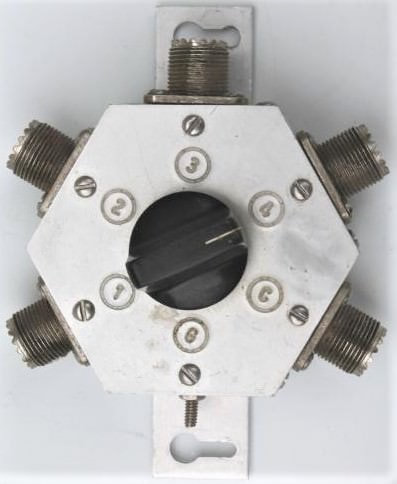
|
with an SO-239 connector on each of five of the sides, and a ground post on the sixth side. The way the unit is designed, when a given position is selected, all of the other positions’ connectors are grounded. The connectors are labeled “1” through “4”, “C”, and “G”. The internal switching mechanism has no physical stop, which means that it can be rotated a full 360° if so desired.
The complaint was that positions “3” and “4” were defunct, with no connection to the common connector or to ground when selected. At first, it seemed like a straight-forward open circuit problem, such as a broken solder joint at each of the non-working connectors. Close examination, however, showed that all of the solder joints were intact. On the off chance that there were hidden defects there, I went ahead and reflowed the solder on all of the connectors, but to no avail. The problem still existed.
I decided that the problem had to be inside the switch itself, so I disassembled the unit, de-soldering all of the connectors from the switch. The switch is a double-sided rotary switch on a ceramic substrate, with a contact disc on either side of the ceramic base, and a fixed brush at each of the connector positions. In its assembled condition, only the ground side of the switch substrate or base is visible; the detent plate at the top conceals the upper active connection disc and brushes.
This meant that I would need to disassemble the switch to get at the upper contact disc. No problem — it is held together by a pair of machine screws with spacers, washers, and nuts. Once the switch was apart, I began to investigate just why there was no continuity at those two switch positions. What I found was a bit of a surprise. The whole problem was a heavy build-up of oxidation on the brush contacts at those two positions. The fix was fairly simple - some cotton swabs, a toothbrush, and some DeoxIT® Gold. Twenty minutes of cleaning on both sides of the ceramic disc, and the switch contacts were operational again. Another ten minutes, and the switch was reassembled and ready to go back into the unit, with a fresh application of DeoxIT® X10S on the shaft and bushing to aid in long-life operation.
I cleaned up all of the parts, including wire-brushing the threads on the SO-239 connectors. Then I re-assembled the entire unit, and soldered the connectors to the switch terminals. Testing with an ohmmeter showed good clean continuity and zero resistance through all positions of the switch. Passing 30 VDC through the switch from common to each output in turn showed zero voltage drop internally in the switch.
So what happened here? Why did only two of the switch positions have this heavy oxidation? As it turns out, the owner has had this switch in service for over thirty-five years, but he has never used anything but switch positions “1” and “2”, and never turned the switch all of the way around the dial - he simply switched it back and forth between the two positions he used. This led to a lack of “scrubbing” at the unused positions, and age and time took over from there.
Moral of the story? Sometimes, it pays to take the long way around. Exercising the switch through its entire range of travel from time to time will help to keep the contacts clean and oxidation free, allowing the switch to perform up to it design specifications. See you next month!