|
Pacific Antenna Buddy Keyer & Speaker Console |
Pacific Antenna Buddy Keyer and Speaker Console Kit Build
By Chris Prioli, AD2CS
I am back in the build shop again, and this time it’s another kit from the Pacific Antenna folks at www.qrpkits.com. The kit (Figure 1) arrived after a short delay in order processing, and it turned out to be a simple and straightforward build. Before we get into the build itself, let’s talk a little bit about the details of the unit.
The Basics of the Buddy Keyer
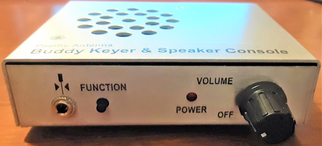
The Buddy Keyer, shown above, is meant to serve as an interface between a paddle and a radio without an internal keyer function. This unit is small! It measures only 4” x 4” x 1”, including the volume knob protuberance. The printed circuit board (PCB) is a mere 2.5” long x 1” wide (Figures 3A and 3B). It lives in a two-piece brushed aluminum enclosure that has a fairly rough surface finish. In fact, the surface finish is too rough to properly accept the water-slide decals that are supplied as labeling for the unit. More about that later.
The unit is designed with two memory channels, each of which will hold up to 29 characters. This lets the user pre-define a couple of standard CW messages and store those messages against future repeated use. For example, you might want a standard CQ greeting, or maybe a QTH string. Twenty-nine characters per memory channel is the limit.
The unit includes an 8Ω 500mW 2” speaker, allowing the user to hear what has been keyed into the unit, or to hear the audio output of the connected transceiver. This speaker, together with the removal of an internal NST jumper, allows the use of the unit as a stand-alone code practice oscillator with the addition of your paddle.
The ATTiny13 microcontroller provides for the basic operating properties of the keyer :
- As already mentioned, two 29-character memories
- Speed adjustable from 5 to 40 words per minute
- Beacon mode
- Sleep mode to drop current draw when not active
- Low general power consumption, on the order of 10mA RX and 20mA TX
The whole thing is powered by a standard 9-volt snap-top battery - something else that we will discuss further later on. Kit build time was about an hour, not counting paint drying time. This unit is an ideal accessorial match for any rig that is “earphone only / key only” in design, as it provides the rig with a keyer function as well as a speaker function via an integrated LM386 audio amplifier implementation.
The front panel carries the paddle input jack, a function control pushbutton switch, a “power good” indicator LED, and the ganged power switch/volume control. In its default configuration, the rear panel carries a keyer output jack for connection of the keyer to the transceiver key input jack, and an audio input jack for connection of the keyer audio amp to the transceiver headphone output jack. As built, however, the rear panel also carries a coaxial DC power jack for the introduction of nominal 12VDC power, widely available in the typical shack. Again, we will discuss this in more detail a little bit later.
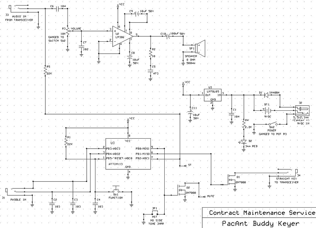
Refer to the schematic diagram featured above. The circuits that comprise this unit are fairly simple but at the same time quite elegant. Because of its commonality, we will start out with the power supply. At one time in its design history, the unit was intended to have a DC input jack for 12.0 to 13.8 VDC input. It has since been removed from the manual, the schematic as published in the manual, and the kit contents. However, I wanted that flexibility, and I wanted not to have to worry about weak or dead battery problems. As a result, I added the power jack back into the unit, using a metallic bodied coaxial DC power jack with a switch on the ground circuit. It was easy to see how and where this jack was originally connected to the power supply circuit, and the wire connect points and traces were still there on the PCB, so it was really a no-brainer.
The jack input and the battery are basically parallel to each other, with the unit power switch between the battery or jack negative terminal and chassis ground. A 1N4004 diode bypasses the battery when the power is supplied via the jack. From the battery positive terminal and the diode cathode, we go into the input of the LM78L05 voltage regulator IC. However, there is a 0.1µF filter capacitor to ground at the v/reg input, and the input lead is also connected to a 2.2K limiting resistor and the 3mm red LED used as a pilot lamp. The voltage regulator output is wearing a 10µF electrolytic capacitor to ground to limit high-frequency noise in the output, and becomes the circuit Vcc supply point. Vcc is supplied to Pin 6 of the U2 LM386 amplifier IC and to Pin 8 of the U1 ATTiny13 8-bit microcontroller.
The audio amplifier is basic, with the input signal coupled to the non-inverting input at Pin 3 through the 10KΩ volume control. The output from Pin 5 is fed to the loudspeaker via a 100µF electrolytic capacitor.
The microcontroller uses the paddle “dit” and “dah” leads as two of its inputs, each of which is bypassed by a 0.01µF capacitor. Another input is the Function pushbutton switch, which also carries a 0.01µF bypass cap to ground. There is also a selectable control for the sidetone. The µC outputs are the key stream to the transceiver and the side tone signal.
The Build
Before beginning the actual assembly, I chose to prep the enclosure halves for decaling, and then to apply the decals. This was so that the enclosure would have plenty of time to dry completely before I began installing components to it.
The prep consisted of scrubbing the metal with a medium Scotch-Brite® pad, working with the grain of the metal. Once the metal was as smooth as I could get it, I cleaned it off with some 99% isopropanol, letting it air dry completely before continuing. The next step was a pair of light coats of fast-drying clear enamel spray, allowing each coat to dry thoroughly before applying the next one.
Once the second coat has dried, the decals can be applied to the enclosure. The kit ships with two complete sets of decals just in case of a goof. Careful handling prevents goofs. Follow the graphics shown on Page 11 of the Buddy Keyer Console instruction manual. You will note that there are a couple of decals on the sheet that are not shown in the Page 11 drawings. This is because there was a running change made to the kit at some point, deleting a DC power jack from the unit. As explained in more detail later on, I chose to incorporate this jack back into the unit, and installed it to the right of the earphone jack on the rear panel, and so I also installed those “extra” decals there as well.
The decals are applied by first cutting them apart from the master sheet, cutting carefully around each decal. One by one, place each decal into a dish of warm water into which a drop of dish soap has been added to break the surface tension of the water. About ten seconds or so after immersion in the water, the decal will be able to slide freely off the backer sheet. Carefully slide the decal off the sheet and onto the enclosure near its installation location. Using your fingertip, gently move the decal into its final position, and then blot it there using a soft paper towel or facial tissue. Repeat the process for each individual decal until they are all in place and all of the excess water has been blotted off. After allowing several hours for the decals to dry completely, another two light coats of the clear enamel were applied as before.
As is the norm in kit builds of this nature, we started with the lowest-profile components first. In this case, that was the resistors and the ceramic capacitors. Next came the IC sockets. A quick word is due here. My general practice is to socket all IC’s unless there is a specific design reason not to do so. In the case of this kit, it was supplied with only one IC socket - that for IC U1, the microcontroller, with the thinking that the IC may need to be removed for re-programming at some point in the future. No big deal - I would just kick in another DIP-8 socket from my inventory… except that I didn’t have one! Believe it or not, I was out of 8-pin DIP sockets.
Never one to let a simple thing like lack of inventory stop me, I decided to make one out of a 16-pin socket, of which I had plenty. I simply took an open-frame DIP-16 socket and snipped the side rails a little bit behind the fourth slot on each rail, and voilà! This contrivance can be seen in the completed PCB illustration in Figure 5 if one looks closely enough. Look carefully at the left end (opposite the U1 label) of the IC socket and you will see that there is nothing bridging the two rails. This works just fine because once it is soldered onto the PCB, it is as solid as a complete socket would be.
When installing IC sockets, be sure to align the notched end of the socket with the Pin 1 indication on the PCB. This may be a small circle or dot, or a matching notch in the screen printed IC outline, or sometimes just a square pad at the Pin 1 hole in the PCB. The notch in the IC socket will later be used to aid in aligning the IC properly when it is installed in the socket. Because of the fact that I was socketing both IC’s, I did not install the U2 IC at this point as the build instructions would have the builder do. I preferred to hold off until after I could verify the operating voltages on the board.
Next up were the three TO-92P devices - the LM78L05 5V 100mA voltage regulator, and the two 2N7000 enhancement mode N-channel MOSFET’s. These get installed in alignment with their body outlines in the PCB screen printed legend. After the MOSFET’s, I installed the right-angle pushbutton Function switch at the S1 location.
It was now time to install the 1N4004 diode. This diode is installed upright or on end, with the cathode end (the striped or banded end) to the top. This construction technique is usually employed as a space-saving ploy. Sometimes, however, it is used as a means of providing a convenient test point connection at the upper end of the diode (or other axial component).
After the diode, I installed the 2-pin jumper header at the NST location and one of the three stereo TRS jacks at the J1 location. Following the jumper and the jack, electrolytic capacitors C8, C9, C10, and C11 were all installed. C8, C9, and C11 are all 10µF 50V types, while C10 is 100µF 50V device. These capacitors are all polarity-sensitive, so care must be taken to install them correctly. On these caps, the long lead is the positive lead, and the negative lead is clearly indicated on the capacitor body by a broad stripe.
The next step was the only tricky part of the build. The installation of the 3mm red LED used as a pilot lamp/power good indicator required that the LED leads be bent 90° at a certain point along the length of the leads. The idea is to bend the LED leads so that the leads are folded down at a distance of 3/16” from the back of the LED body, and then to solder it in place so that the mid-line of the LED body is 1/4" above the PCB top surface. When bending the LED leads, it is important to verify that the LED polarity is correct, so that the cathode lead (next to the flatted side of the LED) goes into the proper PCB hole, next to the flatted side of the screen printed LED outline. The specific positioning of the LED is important, as the LED must fit into a machined hole in the enclosure lower half when the PCB is installed. This completes the component-level assembly of the printed circuit board. As stated above, Figure 5 illustrates the board at this point in the build.
Next up was the installation of the speaker to the chassis upper half. The kit included a pair of 4-40 x 3/8” flat head machine screws and two speaker clamps. I assembled the clamps to the enclosure cover by placing the screws in the holes and then threading the clamps onto the screws with the short leg of each clamp towards the sheet metal. Sliding the speaker under the long side of the clamps, I then tightened the screws to bring the clamps down onto the speaker rim. See Figure 6.
Next, it was necessary to install a three-inch length of hook-up wire to each of twelve wire connect points along two edges of the PCB, five of them along the short end of the board nearest to the U2 IC at the R3 and S2 locations, and the other seven along the long edge directly opposite the J1 stereo TRS jack at the J2, J3 and J4 locations. After these wire leads are installed to the PCB, install the battery snap connector to the board at the BATT location , with the red wire to the “+” hole and the black wire to the “-“ hole. Finally, install the speaker wires to the PCB at the SPKR location, with the red wire in the hole over the “R” in “SPKR”. Note that you may have to clip off a plug from the speaker wire pair. At this point, the PCB is ready for installation into the chassis lower half. Figure 7 shows the installed speaker in the upper enclosure half and the wired PCB ready for installation into the chassis.
Now it was time to begin installing components into the lower chassis or enclosure half. I began by marking and center-punching the hole center for the DC power jack. This required the drilling of a 5/16” (8mm) hole in the chassis rear surface. Once that was done, I started by installing the four self-stick rubber feet to the underside of the lower enclosure half. This helped to keep the enclosure from sliding on the work surface when soldering to the chassis-mounted components. I then installed the DC power jack and the two stereo TRS jacks. For soldering access, the DC power jack went in with its terminals at nine o’clock, twelve o’clock, and three o’clock, and the TRS jacks went in with their wire terminals up. The power jack was secured with a hex nut, and the other jacks with round knurled nuts. Next to go in was the volume control/on-off switch assembly. I carefully folded all five terminals ninety degrees, so that they would be pointing straight back and ready to both accept wiring and clear the upper chassis half when it is installed. Figure 8 shows the lower chassis half just before folding the terminals on the on-off/volume control.
I was then ready for the installation of the PCB into the chassis. Unfortunately, the retaining screws for the PCB were not included in the kit. Back to my inventory, this time for a pair of 4-40 x 1/4” Phillips pan head machine screws and a pair of #4 internally-toothed lock washers. The PCB fits nicely into the front left corner of the chassis, with the paddle jack, the function switch, and the LED all fitting into mating holes in the chassis front panel. It was a simple matter to put the PCB into place and then to install the two retaining screws with lock washers to secure the PCB. I then installed a round knurled nut onto the paddle jack.
It was now time to wire everything up. I started with the volume control’s three wires. The wire connect points on the PCB are numbered 1, 2, and 3. The middle three of the five terminals on the control are for the volume potentiometer. Looking down at the control from above as viewed with the front panel of the chassis towards you, Pin 1 is the right-most of the center group of three, Pin 2 is the center terminal, and Pin 3 is the leftmost of the group. Simply connect the wires from the like-numbered points on the PCB to these terminals on the control. Next, connect the two switch wires from the S2 location of the PCB to the remaining terminals on the control. It does not matter which wire goes to which terminal.
Moving to the wires along the long edge, these will get connected to the jacks on the rear panel. In my case, because I installed the DC power jack, I had a total of seven wires to connect, three to the DC power jack, and two each to the TRS jacks.
Starting with the DC power jack, the “+” wire goes to the terminal that ties to the center pin. The two remaining wires will go to the negative terminal and the switch terminal, as marked on the PCB.
The two TRS jacks are wired the same way, using the “S” or sleeve terminal and the “T” or tip terminal. When viewed from the inside of the chassis, J4 is the right-hand or Key jack, leaving J3 as the left-hand Audio one. In each case, the “TIP” wire from the PCB will go to the “T” terminal on the jack, and the “G” wire will go to the “S” terminal of the jack.
As all else was ready, I moved on to the voltage tests. I connected a 9V battery to the snap connector, and with my DVOM ready, I powered on the unit. The LED came on, as was expected. I then checked for +5VDC at Pin 8 of U1 and Pin 6 of U2, both with respect to ground, and found the voltages to be OK. I powered the unit down and removed the battery temporarily, long enough to install the two IC’s in their respective sockets, paying careful attention to the Pin 1 or notch orientation. Figure 9 shows a close-up view of the assembled and tested PCB in place in the chassis. A final look-over to make sure that there were no crossed wires and that all of the soldering was secure, and the cover was ready to go on.
Following one more photo opportunity (Figure 10), the cover was installed to the unit, securing it with the two supplied 4-40 x 1/4” flat head machine screws. This completed the build of the Pacific Antenna Buddy Keyer and Speaker Console. The completed unit is shown in Figure 11.
Conclusion
Use of the Buddy Keyer and Speaker Console with your radio requires the use of two stereo jumper cables, male to male with 1/8” (3.5mm) plugs at each end. One of these is connected from the radio’s “key” jack to the “key” jack on the keyer and the other runs from the radio’s “headphone” jack to the keyer’s “headphone” jack. The assumption is made that your rig’s input and output circuits are between the tip and sleeve of the respective jacks. If your rig uses the ring connection instead of the tip, adjustment will need to be made, either by customizing the cable(s) as needed, or by re-wiring the J3 and J4 jacks in the keyer to match the radio function. Remember though that this will then be a non-standard keyer, usable only with that specific radio model or series of like-wired sets.
Let’s talk about the NST jumper for a minute, This is the No SideTone jumper, and it is used as follows :
- If your radio generates its own sidetone internally, install the jumper to turn off the keyer sidetone function.
- If your radio does not generate its own sidetone internally, stow the jumper on a single pin of the header, leaving the NST circuit open and enabling the keyer’s sidetone function.
- If you want to use the keyer as a code practice oscillator together with a paddle set, remove and stow the jumper as above.
Remember to always power down the keyer before changing the jumper position! This is important to prevent damage to the microcontroller in the keyer. Note also that the ST and MUTE points in the keyer are no longer used. They were once parts of an earlier design that used this circuit board.
There are five basic keyer functions, which are selectable using the front panel Function switch :
- Send message
- Set code speed
- Enter/Exit tune mode
- Enter store message mode
- Change between Iambic B and A modes
The unit assembly instruction manual provides complete operational instructions for the keyer unit. The manual is well-written and is quite easy to follow, both for the build instructions and for the operation of the unit afterwards. I was quite happy with the compact size of this unit, and I think that it was a mistake to remove the 13.8V power option from the standard kit, as every ham has a quarter of an amp or so of 13.8V power available on the shack desk, right?
All things considered, I would rate this one an A-, and the minus is only because of the removed DC jack and the missing screws.
One final note. Look carefully at the image in Figure 11 and compare it with Figure 2 photo. Did you notice the difference? The Figure 11 image came from the Buddy Keyer user manual front page, while the Figure 2 photo came from my build. It is my guess that the design changes that led to the dropping of the DC power jack and the disuse of the MUTE and ST connections happened at the same time that the decal set changed...