|
80M/160M Dual-Band QRP Transceiver |
80m/160m Dual-Band QRP Transceiver Kit Build
By Chris Prioli, AD2CS
Almost immediately upon getting my ham ticket (which I did in spectacular fashion - more about that later), I was given some radio kits that other hams had purchased but for one reason or another failed to build. One of the kits is a BITX-40 40-meter transceiver kit, which comes as an assembled board that simply needs to be installed into an enclosure, have its off-board components installed to the chassis, and be wired up. Easy-peasy! The other two kits are bare-board kits, one of which is a 75-meter transceiver with phone and CW modes, and the third one is a dual-band 80-meter/160-meter CW transceiver. All of these kits are low-power rigs. This article will describe the build process for the dual-band CW rig. Figure 1 shows the parts kit as unpacked.
This radio build included the placement of thirty-four resistors, one trimpot, fifty-six capacitors (of which nine are electrolytics), eight IC sockets (seven of which are populated by IC’s, more about the last one later), a relay, three tactile switches, twelve assorted transistors, two voltage regulators, four assorted diodes, three RF chokes, one rotary encoder, five toroidal coils, and one toroidal transformer. Of course, the toroids all need to be wound at the time of building the rig. There is also an AD9834 DDS daughterboard installed to the mainboard.
External to the board and chassis-mounted are a power switch/volume control pot, a 16x2 LCD panel (both to the front panel), a power jack, a headphone jack, a paddle/key jack, and two antenna jacks (all to the rear panel). An 8 ohm ½W speaker mounts to the enclosure top cover.
The kit includes a double set of waterslide decals for the front and rear panel features as well as a formed aluminum rod bail that is installed to the chassis bottom and used to elevate the front of the radio on the desktop. One poor feature is the fact that the rubber feet included in the kit are not tall enough to lift the bail brackets on the chassis bottom clear of the desktop when the bail is closed. The surface finish of the enclosure is not amenable to the direct installation of the decals. As a result, some surface prep is necessary. I scrubbed the surfaces smooth using a ScotchBrite® pad and working with the grain of the metal. Next, I cleaned the aluminum with some 99% isopropyl alcohol. Once dry, I applied two light coats of a clear matte enamel spray, allowing the finish to dry completely between coats. After the decals were installed, I once again applied two light coats of the clear matte enamel spray as before.
Assembly hints, schematics, and board layout diagrams as well as bail and decal instructions are all available at http://qrpkits.com/mbdc.html. There are no detailed assembly instructions provided, so this kit is not really one for a beginner. Some experience in identifying components is necessary, as is substantial skill in soldering. While not difficult, some patience is required for winding the toroids. Good instructions for this task are provided, so no worries there! The MBDC kit sells for $200.00.
OK - on to the build…
Day 1
I started out by separating all of the resistors and sorting them by value. The online manual, which I printed for convenience, provides the resistor color codes for those who are not familiar with resistor color coding. However, for some builders, that help will only be useful up to a certain point. I don’t know if the standard kit complement is made up this way or not, but about a third of the resistors in my kit were not the standard
1/4W-5% 4-band carbon film resistors used throughout this kit. Instead, there were a handful of 1/8W-1% 5 band metal film types. While the color code is basically the same, the translation scheme does change slightly. For example, a 47kΩ (kiloohms) 1% resistor becomes Yellow-Violet-Brown-Red-Brown instead of Yellow-Violet-Orange-Gold. Nothing in the build notes suggested that the resistors had been changed as a design change, so I made the working assumption that the difference in resistor types was more of a parts-on-hand issue when the kits were being gathered and prepped. For power capacity uniformity and because I want the rig to match the build sheet if/when I eventually sell it, I replaced all of the 1/8W-1% resistors with 1/4W-5% types from my inventory.
Take care when sorting the resistors. The three RF chokes are similar to resistors in size and appearance, and the 10Ω resistor and the 10µH(microHenrys) RF choke even have the same color codes. The RF chokes are, however, considerably and visibly larger than the ¼W resistors supplied with the kit. Another likely area of confusion is between the 51Ω resistor and the 1MΩ resistor. The 51Ω resistor carries a color code of GRN-BRN-BLK-GLD, while the 1MΩ(mega-ohms) resistor is color-coded Black-Brown-Green-Gold. If you are unsure of the value based on the color code, use an ohmmeter to check the measured resistance of your resistors. When doing this, however, don’t expect the measured value to be exactly the nominal value of the resistor. The gold fourth band tells us that the resistor will be within ±5% of the nominal value, meaning that the 1MΩ device can measure anywhere from 950kΩ to 1050kΩ (1.050MΩ). On the other hand, the 10Ω resistor can measure anywhere from 9.5Ω to 10.5Ω. Remember - you are only using the ohmmeter to confirm your color-code translation.
The resistors are all formed to a 0.4” lead pitch. I have one of those plastic lead forming tools, so it was a breeze to get uniform bends on the resistors. With the PCB mounted in my PCB fixture with the component side up, I placed all of the resistors, working with about five of them at a time. Without flipping the PCB, I soldered the just-installed resistors working from the top of the board, but not cutting excess lead lengths yet. After soldering those five resistors, I added the next five and soldered them in the same manner, again leaving the tails intact. I repeated this process until all thirty-four resistors had been placed.
Next, I flipped the board over and began doing touch-up soldering and clipping of the resistor leads. “Touch-up soldering” refers to resoldering, from the foil side, any leads that do not appear to have been adequately filled and bonded when soldered from the top. Start at one corner and work your way across the board until you have checked and clipped every resistor lead. Inspect your work carefully, checking for shorts (solder bridges, etc.), and also for loose or unsoldered leads.
I followed up the resistor installs by placing the diodes - two 1N5817 Schottkys, one 1N4756A 47V Zener, and one 1N4148 general-purpose diode, aligning the cathode end of each diode as marked on the PCB. After the diodes, I installed the three axial RF chokes.
In keeping with the traditional methodology of installing components shortest to tallest, I sorted and installed the disc and film capacitors next. Out of the forty-seven capacitors installed in this group, twenty-one are of one type - a 0.1µF(microFarad) (104) MLCC type. There are five 0.01µF (103) film capacitors, nine 0.001µF (102) disc capacitors, one 100pF(picoFarad) (101) disc capacitor, and two 470pF (471) disc capacitors. The astute reader will have noticed that this listing accounts for only thirty-eight of the total forty-seven non-polarized capacitors. Here’s why…
Remember that this rig was described up front as a “dual-band” unit? The designer of this kit chose to make the band selection something that the builder should decide upon at build time. Along the right edge of the PCB, with the board oriented so that the encoder and tact switch positions are towards you, there is an area bordered by a heavy white line. The bordered area is divided into two sections. Within those sections are the labels “Band A’ and ’Band B’. Band A has locations for two toroidal coils and four capacitors, while the Band B section has locations for two toroidal coils and five capacitors. These, then, are the missing nine capacitors. The values of these capacitors will change based upon the specific bands chosen for the radio. Similarly, the windings of the toroidal coils, and in fact the toroids themselves, will also change by band.
My original plan was to build this set as a 20-meter/40-meter unit, but once I realized how busy those bands can get, I decided to build it out as designed, for 80 meters / 160 meters. This meant installing nine C0G MLCC capacitors - one 150pF, one 220pF, two 680pF, and five 1500pF. Time for a photo break. See Figure 2.
The nine electrolytic capacitors were next, minding the polarity of each capacitor , followed by the eight IC sockets, taking care to align the notches in the sockets with the notched ends of the IC socket images on the PCB. On this go-round, I also installed the DIP relay.
Now it is time to install the assortment of transistors and the voltage regulators. The transistors include one J175 P-channel J-FET, two 2N3904 general purpose NPN bipolars, five 2N7000 N-channel enhancement mode MOSFETS, three BS170 N-channel enhancement mode MOSFETS, and one FQP8P10 P-channel power MOSFET. All transistors except the FQP8P10 are in TO-92 cases, as is the LM78L09 9-volt voltage regulator. Both, the FQP8P10 MOSFET and the LM7805 5-volt voltage regulator are in TO-220 cases. Care must be taken to get all of these semiconductor devices into their proper and correct location. After the transistors and regulators were installed, I also installed the rotary encoder, the trimpot, and the three tactile switches before taking a photo break. See Figure 3.
It was time to move to the chassis for a few minutes, as I was almost ready to knock off for the night, and I wanted to start pretty fresh when I began winding the toroids. So, I decided to install the chassis front and rear panel features, the wire bail, and the loudspeaker. The front panel got the on-off/volume control combo, while the rear panel got the two antenna jacks, the DC power jack, the paddle/key jack, and the headphone jack. These are all straightforward, but remember to bend over (or break off) the locator tab on the front panel pot. I took a photo of all of that (See Figure 4), and then came the installation of the brackets and bail to the chassis bottom surface, together with the four self-adhesive rubber feet, (See Figure 5). That completed the main chassis prep, so it was time to move on to the loudspeaker.
The speaker is mounted to the cassis top cover by way of two small L-shaped clamps and some 4-40 hardware. The clamps are placed on the rim of the speaker and the hardware is tightened to keep everything in place. I suggest positioning the wire leads so that they are pointing towards the center of the enclosure rather than towards the periphery. Photo time again! See Figure 6.
I now began to see, in my mind’s eye, the mainboard installed into the chassis, and I realized that I was not comfortable with the lack of additional cooling for the output transistor or the 5V voltage regulator, so I set out to do something about it. Although the design did not include them, I added simple anodized aluminum heatsinks to both of these TO-220 devices. One of these heatsinks - the one on the output transistor - required some minor modification. As can be seen in the photo in Figure 11, the “wings” of the heatsink were spread slightly, and somewhat more on the right side, so as to provide clearance between the heatsink and the TX/RX antenna jack. It was for this reason that the stamped anodized type of heatsink was chosen for this task rather than the extruded type. I wanted the “bendability” of the stamped heatsink.
I rounded out the day by wiring up the LCD panel to the mainboard. The kit included a length of 16-wire zip-type ribbon cable, which is used for the LCD hook-up. First, we strip off a 6-wire strip from the whole, and then we strip off another 4-wire strip. This leaves a six-wire leftover strip, of which we will use a small piece later. The two strips that were separated from the whole need to have their individual leads separated for about 3/4" at each end, with each lead then having 1/4" of its insulation stripped off. The stripped leads all get tinned, at both ends of the two cables. Now, using the 6-wire strip, insert the wires in order into holes 1 through 6 on the LCD panel, and then solder them in place. Using the four-wire strip, insert the wires, in order, into holes 11 to 14 of the LCD panel, and solder them in place as well. Now move to the other end of these cables, soldering wires 1 through 6 in order into holes 1 through 6 on the “LCD PANEL” pad on the mainboard, followed by soldering wires 11 through 14 in order into holes 11 through 14 in the mainboard “LCD PANEL” pad. Take care not to cross any of these wires. Finally, strip off one of the remaining wires in the scrap 6-wire strip, and then cut (2) two-inch lengths of wire from that single length. Strip about ¼" of insulation from each end of each wire, and tin those stripped ends. Finally, place and solder these wires as jumpers from Pin 1 of the LCD panel to Pin 16, and from Pin 2 to Pin 15. This provides power to the LCD panel backlight system. A couple of photos (See Figure 7 and Figure 8), and then I called it quits for the day.
Day 2
The first task for today is to wind the toroids. Just because it was different, I decided to start with the T1 transformer. This job required the use of a folded-over and lightly twisted length of magnet wire, which is passed through the toroid the stated number of passes, or “turns”. Each time the wire passes through the core of the toroid, it is counted as a “turn”. In this case, six turns were specified. When winding the toroids, always leave about 3/4" of wire extending out of the core at each end of the coil. This winding becomes a transformer by first snipping apart the closed end where the wire was folded. Next, strip off the enamel coating of the magnet wire almost all the way to the toroid, stopping about 1/8” from the toroid.
Stripping is best accomplished either with some 400-grit sandpaper, or - my preferred method - by dragging a ball of molten solder on the soldering iron tip along the lead until the coating is melted off and the wire is tinned. This method takes only a few seconds per lead, and leaves you with a clean, tinned lead ready for insertion into the PCB. Once all four leads of this toroidal transformer are tinned, it is time to identify and separate them into a primary and a secondary winding. This is easier than it sounds, and only involves the use of a continuity tester or an ohmmeter. Start with one tester lead clipped to any one of the leads. Next, touch the opposite tester lead to each of the leads at the opposite end of the coil until you find the one that has continuity to the first lead. This will be your primary winding, with the other pair of leads comprising the secondary winding. Arrange the leads as shown in the build notes for insertion into the PCB. Insert these leads into their appropriate holes in the PCB, gently pushing the toroid down to the PCB, and then solder the leads in place. If done properly, the coated portion of the wire will be just above the PCB top surface.
Once the transformer is done, the other toroids will seem easy by comparison. Yes, there are more turns needed, but that’s just a matter of counting. Once the full number of turns has been laid down onto the toroid, and again with 3/4" of wire extending at either end of the coil, strip and tin the leads as before. As you wind these coils, remember to keep track of which one is which, and make sure that you are using the correct toroid for each coil in turn. In the standard 80-meter/160-meter version of this rig, four of the toroid forms are identical, so the only difference between the finished coils is the number of turns of wire laid down for each coil. You can either install each one as it is wound, or you can wind them all and then install them all at once. Either way, press each coil down gently against the PCB when soldering the toroids in. In every case, the turns should be spaced evenly around the toroidal ring, should fit the ring fairly closely, and should only have tinned wire extending through the PCB before soldering. After the toroids are all installed, a spot of hot glue at the base of each toroid will secure them to the PCB. Time for another photo. See Figure 9.
It is now time to move on to the remaining wiring from the mainboard to the various controls and features. The build notes provide wire connection graphics, showing which wires go where. I did not use the hook-up wire that came with the kit, preferring instead to use my own hook-up wire whereby I could select wire gauges and colors as appropriate for each connection. Pairs of wire leads going to a single point should be lightly twisted together, and where possible, the wires should be cut long enough to be routed beneath the PCB when installed in the chassis. Note that the paddle/key jack and the headphone jack are not interchangeable. The headphone jack is a switched jack intended to allow current to reach the speaker when no headphone is in use, but to silence the speaker when a headphone plug is inserted. Time for another photo break! See Figure 10.
Once all of the off-board wire leads have been soldered to the mainboard, it is time to install the mainboard into the chassis. Secure the chassis using four of the screws provided, and also secure the LCD panel to its mounting bosses using the remaining four screws. Then, connect and solder each off-board wire to its proper connection point as shown in the build notes. Remember to keep the wire pairs, and especially the antenna leads, twisted together along their lengths. Figure 11 shows the PCB installed in the chassis bottom.
Using a fused power line or a 1-amp current-limited power supply, power up the rig and check for operation of the LCD backlight. If the backlight comes on, power down the rig and proceed with the assembly. If the backlight does not come on, it is time for some troubleshooting, particularly as regards the 5V supply.
If the backlight is OK, continue by inserting all seven IC’s into their sockets, observing the notched or Pin 1 end of the IC, aligning that end of the IC with the notched end of the IC socket. Use the build notes graphics to identify the location of each IC. Take care not to allow the IC leads to bend out or to fold under the chip on insertion. Once all of the IC’s are in place (Figure 11), it is time to install the AD9834 DDS module. The kit will have included an eight-pin SIP header. This is to be soldered to the AD9834 with the short end of the SIP header strip going to the AD9834. Once the header is soldered in place, the AD9834 can be inserted into the remaining IC socket, using the Pin 1 to Pin 8 side of the IC socket only. The AD9834 will hang over the ATmega48 microprocessor chip. See Figure 11.
Power up the radio with either an antenna or a dummy load, and check the operation of the controls. On initial power-up, the display should read 3.560.000. If no text is visible, adjust the LCD contrast trimpot on the mainboard until the text is clearly visible. If all is OK here, move on to the transmitter test.
Transmitter Test
Start out by connecting a power meter and a 50Ω dummy load to the TX/RX antenna jack. Using a straight key with a mono plug, power on the unit. Key the transmitter and check the output power, which should be about five watts with a 13.8V supply. Switch bands to 160-meters and check the output power again, which should also be about five watts.
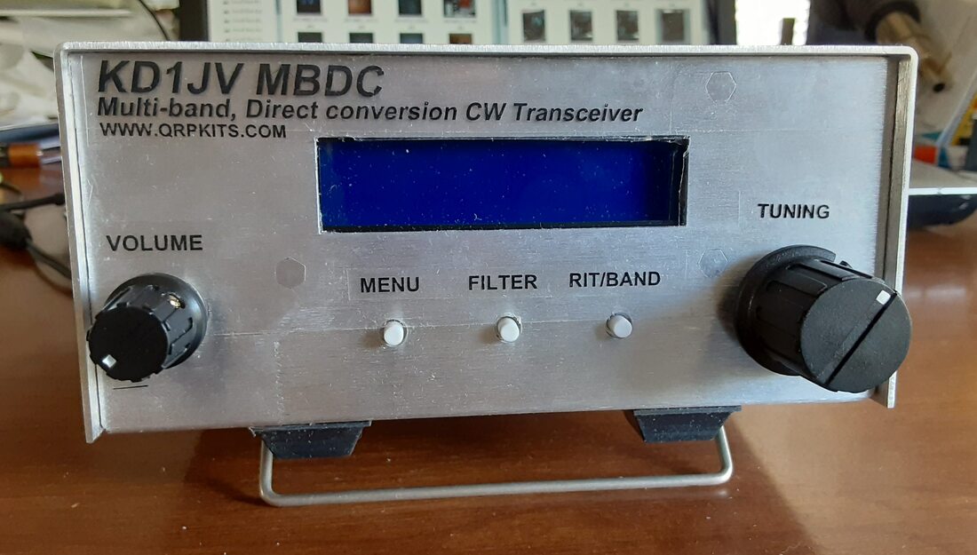
Once all of these tests are passed, the unit is ready for use. See Figure 12. Install the chassis top cover and the job is done! If problems turned up during the testing, refer to the Troubleshooting section of the build notes, which includes a table of anticipated voltages.
This was a fun build that could have been completed in a single day if I had started early enough. As it was, I didn’t get started until late afternoon, so it ran into the second day for me. The build was fairly self explanatory, just pay attention to component values as you place them.
Oh - I almost forgot. About getting my ticket, it seems strange to have a raw beginner carrying an Amateur Extra license, but that is only because I was talked into studying up for all three tests at one time, which I did. I passed all three, so I walked out of my first license test session with an Amateur Extra, and a LOT to learn ahead of me!
By Chris Prioli, AD2CS
Almost immediately upon getting my ham ticket (which I did in spectacular fashion - more about that later), I was given some radio kits that other hams had purchased but for one reason or another failed to build. One of the kits is a BITX-40 40-meter transceiver kit, which comes as an assembled board that simply needs to be installed into an enclosure, have its off-board components installed to the chassis, and be wired up. Easy-peasy! The other two kits are bare-board kits, one of which is a 75-meter transceiver with phone and CW modes, and the third one is a dual-band 80-meter/160-meter CW transceiver. All of these kits are low-power rigs. This article will describe the build process for the dual-band CW rig. Figure 1 shows the parts kit as unpacked.
This radio build included the placement of thirty-four resistors, one trimpot, fifty-six capacitors (of which nine are electrolytics), eight IC sockets (seven of which are populated by IC’s, more about the last one later), a relay, three tactile switches, twelve assorted transistors, two voltage regulators, four assorted diodes, three RF chokes, one rotary encoder, five toroidal coils, and one toroidal transformer. Of course, the toroids all need to be wound at the time of building the rig. There is also an AD9834 DDS daughterboard installed to the mainboard.
External to the board and chassis-mounted are a power switch/volume control pot, a 16x2 LCD panel (both to the front panel), a power jack, a headphone jack, a paddle/key jack, and two antenna jacks (all to the rear panel). An 8 ohm ½W speaker mounts to the enclosure top cover.
The kit includes a double set of waterslide decals for the front and rear panel features as well as a formed aluminum rod bail that is installed to the chassis bottom and used to elevate the front of the radio on the desktop. One poor feature is the fact that the rubber feet included in the kit are not tall enough to lift the bail brackets on the chassis bottom clear of the desktop when the bail is closed. The surface finish of the enclosure is not amenable to the direct installation of the decals. As a result, some surface prep is necessary. I scrubbed the surfaces smooth using a ScotchBrite® pad and working with the grain of the metal. Next, I cleaned the aluminum with some 99% isopropyl alcohol. Once dry, I applied two light coats of a clear matte enamel spray, allowing the finish to dry completely between coats. After the decals were installed, I once again applied two light coats of the clear matte enamel spray as before.
Assembly hints, schematics, and board layout diagrams as well as bail and decal instructions are all available at http://qrpkits.com/mbdc.html. There are no detailed assembly instructions provided, so this kit is not really one for a beginner. Some experience in identifying components is necessary, as is substantial skill in soldering. While not difficult, some patience is required for winding the toroids. Good instructions for this task are provided, so no worries there! The MBDC kit sells for $200.00.
OK - on to the build…
Day 1
I started out by separating all of the resistors and sorting them by value. The online manual, which I printed for convenience, provides the resistor color codes for those who are not familiar with resistor color coding. However, for some builders, that help will only be useful up to a certain point. I don’t know if the standard kit complement is made up this way or not, but about a third of the resistors in my kit were not the standard
1/4W-5% 4-band carbon film resistors used throughout this kit. Instead, there were a handful of 1/8W-1% 5 band metal film types. While the color code is basically the same, the translation scheme does change slightly. For example, a 47kΩ (kiloohms) 1% resistor becomes Yellow-Violet-Brown-Red-Brown instead of Yellow-Violet-Orange-Gold. Nothing in the build notes suggested that the resistors had been changed as a design change, so I made the working assumption that the difference in resistor types was more of a parts-on-hand issue when the kits were being gathered and prepped. For power capacity uniformity and because I want the rig to match the build sheet if/when I eventually sell it, I replaced all of the 1/8W-1% resistors with 1/4W-5% types from my inventory.
Take care when sorting the resistors. The three RF chokes are similar to resistors in size and appearance, and the 10Ω resistor and the 10µH(microHenrys) RF choke even have the same color codes. The RF chokes are, however, considerably and visibly larger than the ¼W resistors supplied with the kit. Another likely area of confusion is between the 51Ω resistor and the 1MΩ resistor. The 51Ω resistor carries a color code of GRN-BRN-BLK-GLD, while the 1MΩ(mega-ohms) resistor is color-coded Black-Brown-Green-Gold. If you are unsure of the value based on the color code, use an ohmmeter to check the measured resistance of your resistors. When doing this, however, don’t expect the measured value to be exactly the nominal value of the resistor. The gold fourth band tells us that the resistor will be within ±5% of the nominal value, meaning that the 1MΩ device can measure anywhere from 950kΩ to 1050kΩ (1.050MΩ). On the other hand, the 10Ω resistor can measure anywhere from 9.5Ω to 10.5Ω. Remember - you are only using the ohmmeter to confirm your color-code translation.
The resistors are all formed to a 0.4” lead pitch. I have one of those plastic lead forming tools, so it was a breeze to get uniform bends on the resistors. With the PCB mounted in my PCB fixture with the component side up, I placed all of the resistors, working with about five of them at a time. Without flipping the PCB, I soldered the just-installed resistors working from the top of the board, but not cutting excess lead lengths yet. After soldering those five resistors, I added the next five and soldered them in the same manner, again leaving the tails intact. I repeated this process until all thirty-four resistors had been placed.
Next, I flipped the board over and began doing touch-up soldering and clipping of the resistor leads. “Touch-up soldering” refers to resoldering, from the foil side, any leads that do not appear to have been adequately filled and bonded when soldered from the top. Start at one corner and work your way across the board until you have checked and clipped every resistor lead. Inspect your work carefully, checking for shorts (solder bridges, etc.), and also for loose or unsoldered leads.
I followed up the resistor installs by placing the diodes - two 1N5817 Schottkys, one 1N4756A 47V Zener, and one 1N4148 general-purpose diode, aligning the cathode end of each diode as marked on the PCB. After the diodes, I installed the three axial RF chokes.
In keeping with the traditional methodology of installing components shortest to tallest, I sorted and installed the disc and film capacitors next. Out of the forty-seven capacitors installed in this group, twenty-one are of one type - a 0.1µF(microFarad) (104) MLCC type. There are five 0.01µF (103) film capacitors, nine 0.001µF (102) disc capacitors, one 100pF(picoFarad) (101) disc capacitor, and two 470pF (471) disc capacitors. The astute reader will have noticed that this listing accounts for only thirty-eight of the total forty-seven non-polarized capacitors. Here’s why…
Remember that this rig was described up front as a “dual-band” unit? The designer of this kit chose to make the band selection something that the builder should decide upon at build time. Along the right edge of the PCB, with the board oriented so that the encoder and tact switch positions are towards you, there is an area bordered by a heavy white line. The bordered area is divided into two sections. Within those sections are the labels “Band A’ and ’Band B’. Band A has locations for two toroidal coils and four capacitors, while the Band B section has locations for two toroidal coils and five capacitors. These, then, are the missing nine capacitors. The values of these capacitors will change based upon the specific bands chosen for the radio. Similarly, the windings of the toroidal coils, and in fact the toroids themselves, will also change by band.
My original plan was to build this set as a 20-meter/40-meter unit, but once I realized how busy those bands can get, I decided to build it out as designed, for 80 meters / 160 meters. This meant installing nine C0G MLCC capacitors - one 150pF, one 220pF, two 680pF, and five 1500pF. Time for a photo break. See Figure 2.
The nine electrolytic capacitors were next, minding the polarity of each capacitor , followed by the eight IC sockets, taking care to align the notches in the sockets with the notched ends of the IC socket images on the PCB. On this go-round, I also installed the DIP relay.
Now it is time to install the assortment of transistors and the voltage regulators. The transistors include one J175 P-channel J-FET, two 2N3904 general purpose NPN bipolars, five 2N7000 N-channel enhancement mode MOSFETS, three BS170 N-channel enhancement mode MOSFETS, and one FQP8P10 P-channel power MOSFET. All transistors except the FQP8P10 are in TO-92 cases, as is the LM78L09 9-volt voltage regulator. Both, the FQP8P10 MOSFET and the LM7805 5-volt voltage regulator are in TO-220 cases. Care must be taken to get all of these semiconductor devices into their proper and correct location. After the transistors and regulators were installed, I also installed the rotary encoder, the trimpot, and the three tactile switches before taking a photo break. See Figure 3.
It was time to move to the chassis for a few minutes, as I was almost ready to knock off for the night, and I wanted to start pretty fresh when I began winding the toroids. So, I decided to install the chassis front and rear panel features, the wire bail, and the loudspeaker. The front panel got the on-off/volume control combo, while the rear panel got the two antenna jacks, the DC power jack, the paddle/key jack, and the headphone jack. These are all straightforward, but remember to bend over (or break off) the locator tab on the front panel pot. I took a photo of all of that (See Figure 4), and then came the installation of the brackets and bail to the chassis bottom surface, together with the four self-adhesive rubber feet, (See Figure 5). That completed the main chassis prep, so it was time to move on to the loudspeaker.
The speaker is mounted to the cassis top cover by way of two small L-shaped clamps and some 4-40 hardware. The clamps are placed on the rim of the speaker and the hardware is tightened to keep everything in place. I suggest positioning the wire leads so that they are pointing towards the center of the enclosure rather than towards the periphery. Photo time again! See Figure 6.
I now began to see, in my mind’s eye, the mainboard installed into the chassis, and I realized that I was not comfortable with the lack of additional cooling for the output transistor or the 5V voltage regulator, so I set out to do something about it. Although the design did not include them, I added simple anodized aluminum heatsinks to both of these TO-220 devices. One of these heatsinks - the one on the output transistor - required some minor modification. As can be seen in the photo in Figure 11, the “wings” of the heatsink were spread slightly, and somewhat more on the right side, so as to provide clearance between the heatsink and the TX/RX antenna jack. It was for this reason that the stamped anodized type of heatsink was chosen for this task rather than the extruded type. I wanted the “bendability” of the stamped heatsink.
I rounded out the day by wiring up the LCD panel to the mainboard. The kit included a length of 16-wire zip-type ribbon cable, which is used for the LCD hook-up. First, we strip off a 6-wire strip from the whole, and then we strip off another 4-wire strip. This leaves a six-wire leftover strip, of which we will use a small piece later. The two strips that were separated from the whole need to have their individual leads separated for about 3/4" at each end, with each lead then having 1/4" of its insulation stripped off. The stripped leads all get tinned, at both ends of the two cables. Now, using the 6-wire strip, insert the wires in order into holes 1 through 6 on the LCD panel, and then solder them in place. Using the four-wire strip, insert the wires, in order, into holes 11 to 14 of the LCD panel, and solder them in place as well. Now move to the other end of these cables, soldering wires 1 through 6 in order into holes 1 through 6 on the “LCD PANEL” pad on the mainboard, followed by soldering wires 11 through 14 in order into holes 11 through 14 in the mainboard “LCD PANEL” pad. Take care not to cross any of these wires. Finally, strip off one of the remaining wires in the scrap 6-wire strip, and then cut (2) two-inch lengths of wire from that single length. Strip about ¼" of insulation from each end of each wire, and tin those stripped ends. Finally, place and solder these wires as jumpers from Pin 1 of the LCD panel to Pin 16, and from Pin 2 to Pin 15. This provides power to the LCD panel backlight system. A couple of photos (See Figure 7 and Figure 8), and then I called it quits for the day.
Day 2
The first task for today is to wind the toroids. Just because it was different, I decided to start with the T1 transformer. This job required the use of a folded-over and lightly twisted length of magnet wire, which is passed through the toroid the stated number of passes, or “turns”. Each time the wire passes through the core of the toroid, it is counted as a “turn”. In this case, six turns were specified. When winding the toroids, always leave about 3/4" of wire extending out of the core at each end of the coil. This winding becomes a transformer by first snipping apart the closed end where the wire was folded. Next, strip off the enamel coating of the magnet wire almost all the way to the toroid, stopping about 1/8” from the toroid.
Stripping is best accomplished either with some 400-grit sandpaper, or - my preferred method - by dragging a ball of molten solder on the soldering iron tip along the lead until the coating is melted off and the wire is tinned. This method takes only a few seconds per lead, and leaves you with a clean, tinned lead ready for insertion into the PCB. Once all four leads of this toroidal transformer are tinned, it is time to identify and separate them into a primary and a secondary winding. This is easier than it sounds, and only involves the use of a continuity tester or an ohmmeter. Start with one tester lead clipped to any one of the leads. Next, touch the opposite tester lead to each of the leads at the opposite end of the coil until you find the one that has continuity to the first lead. This will be your primary winding, with the other pair of leads comprising the secondary winding. Arrange the leads as shown in the build notes for insertion into the PCB. Insert these leads into their appropriate holes in the PCB, gently pushing the toroid down to the PCB, and then solder the leads in place. If done properly, the coated portion of the wire will be just above the PCB top surface.
Once the transformer is done, the other toroids will seem easy by comparison. Yes, there are more turns needed, but that’s just a matter of counting. Once the full number of turns has been laid down onto the toroid, and again with 3/4" of wire extending at either end of the coil, strip and tin the leads as before. As you wind these coils, remember to keep track of which one is which, and make sure that you are using the correct toroid for each coil in turn. In the standard 80-meter/160-meter version of this rig, four of the toroid forms are identical, so the only difference between the finished coils is the number of turns of wire laid down for each coil. You can either install each one as it is wound, or you can wind them all and then install them all at once. Either way, press each coil down gently against the PCB when soldering the toroids in. In every case, the turns should be spaced evenly around the toroidal ring, should fit the ring fairly closely, and should only have tinned wire extending through the PCB before soldering. After the toroids are all installed, a spot of hot glue at the base of each toroid will secure them to the PCB. Time for another photo. See Figure 9.
It is now time to move on to the remaining wiring from the mainboard to the various controls and features. The build notes provide wire connection graphics, showing which wires go where. I did not use the hook-up wire that came with the kit, preferring instead to use my own hook-up wire whereby I could select wire gauges and colors as appropriate for each connection. Pairs of wire leads going to a single point should be lightly twisted together, and where possible, the wires should be cut long enough to be routed beneath the PCB when installed in the chassis. Note that the paddle/key jack and the headphone jack are not interchangeable. The headphone jack is a switched jack intended to allow current to reach the speaker when no headphone is in use, but to silence the speaker when a headphone plug is inserted. Time for another photo break! See Figure 10.
Once all of the off-board wire leads have been soldered to the mainboard, it is time to install the mainboard into the chassis. Secure the chassis using four of the screws provided, and also secure the LCD panel to its mounting bosses using the remaining four screws. Then, connect and solder each off-board wire to its proper connection point as shown in the build notes. Remember to keep the wire pairs, and especially the antenna leads, twisted together along their lengths. Figure 11 shows the PCB installed in the chassis bottom.
Using a fused power line or a 1-amp current-limited power supply, power up the rig and check for operation of the LCD backlight. If the backlight comes on, power down the rig and proceed with the assembly. If the backlight does not come on, it is time for some troubleshooting, particularly as regards the 5V supply.
If the backlight is OK, continue by inserting all seven IC’s into their sockets, observing the notched or Pin 1 end of the IC, aligning that end of the IC with the notched end of the IC socket. Use the build notes graphics to identify the location of each IC. Take care not to allow the IC leads to bend out or to fold under the chip on insertion. Once all of the IC’s are in place (Figure 11), it is time to install the AD9834 DDS module. The kit will have included an eight-pin SIP header. This is to be soldered to the AD9834 with the short end of the SIP header strip going to the AD9834. Once the header is soldered in place, the AD9834 can be inserted into the remaining IC socket, using the Pin 1 to Pin 8 side of the IC socket only. The AD9834 will hang over the ATmega48 microprocessor chip. See Figure 11.
Power up the radio with either an antenna or a dummy load, and check the operation of the controls. On initial power-up, the display should read 3.560.000. If no text is visible, adjust the LCD contrast trimpot on the mainboard until the text is clearly visible. If all is OK here, move on to the transmitter test.
Transmitter Test
Start out by connecting a power meter and a 50Ω dummy load to the TX/RX antenna jack. Using a straight key with a mono plug, power on the unit. Key the transmitter and check the output power, which should be about five watts with a 13.8V supply. Switch bands to 160-meters and check the output power again, which should also be about five watts.
Once all of these tests are passed, the unit is ready for use. See Figure 12. Install the chassis top cover and the job is done! If problems turned up during the testing, refer to the Troubleshooting section of the build notes, which includes a table of anticipated voltages.
This was a fun build that could have been completed in a single day if I had started early enough. As it was, I didn’t get started until late afternoon, so it ran into the second day for me. The build was fairly self explanatory, just pay attention to component values as you place them.
Oh - I almost forgot. About getting my ticket, it seems strange to have a raw beginner carrying an Amateur Extra license, but that is only because I was talked into studying up for all three tests at one time, which I did. I passed all three, so I walked out of my first license test session with an Amateur Extra, and a LOT to learn ahead of me!